Plasma processing apparatus and plasma processing method

a plasma processing apparatus and plasma technology, applied in the field of plasma processing apparatus and plasma processing method, can solve the problems of non-uniform radial direction of process characteristics, achieve the effect of preventing or suppressing undesired films, improving plasma density spatial distribution characteristics or sputtering effects, and improving in-surface uniformity of processes

Active Publication Date: 2007-10-11
TOKYO ELECTRON LTD
View PDF8 Cites 35 Cited by
  • Summary
  • Abstract
  • Description
  • Claims
  • Application Information

AI Technical Summary

Benefits of technology

[0008]It is, therefore, an object of the present invention to provide a capacitively coupled plasma processing apparatus and method of a dual frequency application type in which two kinds of radio frequency powers are applied to an electrode for supporting a target substrate thereon, wherein in-surface uniformity of processes can be improved by controlling plasma density spatial distribution characteristics while preventing or suppressing an undesired film from being formed on another electrode facing the electrode for supporting the target substrate.
[0014]Due to the high impedance at the first radio frequency, the first radio frequency current hardly flows from the second electrode to the first electrode. Accordingly, there is relatively increased a portion of an electron current in the plasma flowing in the sidewall of the processing chamber, which makes the plasma density widen in the outwardly radial directions. In this way, by optimally increasing the impedance at the first radio frequency in the parallel LC circuit, plasma density spatial distribution characteristics can be controlled to be uniform diametrically. Meanwhile, by decreasing the impedance at the second radio frequency in the parallel LC circuit, the ions in the plasma which vibrate according to the second radio frequency are incident onto the first electrode with a strong impact. As a result, an undesired film adhered to a surface thereof can be effectively sputtered (removed) therefrom.
[0017]In the third and the fourth aspect of the present invention, an equivalent circuit in a radio frequency transmission line from the boundary surface between the processing space and the first electrode to the ground potential via the first electrode is configured as a serial-parallel LC circuit. In this serial-parallel LC circuit, an impedance extremely decreases at a specific frequency (resonance frequency) and extremely increases at another specific frequency (antiresonance frequency). By utilizing those characteristics, a high impedance and a low impedance can be obtained at the first and the second radio frequency, respectively. In accordance with an embodiment of the present invention, the resonance frequency is obtained within a range from about 0.1 kHz to about 15 MHz and the antiresonance frequency is obtained within a range from about 5 MHz to about 200 MHz in the frequency-impedance characteristics of the equivalent circuit or the serial-parallel LC circuit. By optimally increasing the impedance at the first radio frequency in the serial-parallel LC circuit, plasma density spatial distribution characteristics can be controlled to be uniform diametrically. Further, by decreasing the impedance at the second radio frequency in the serial-parallel LC circuit substantially to a level at which a short-circuit occurs, the sputtering effect of removing an undesired film from the surface of the first electrode can be further enhanced.
[0019]In the plasma processing apparatus in accordance with the fifth aspect of the present invention, since a desired DC voltage is applied from the DC power supply to the first electrode via the filter to obtain acting effects thereby. Further, the functions of the first and the second radio frequency can be corrected, controlled or assisted by the frequency-impedance characteristics of the filter. For example, when the filter is provided in the serial-parallel LC circuit as in the second plasma processing apparatus, it is possible to improve the plasma density spatial distribution characteristics or the sputtering effect for the first electrode (which removes an undesired film therefrom).
[0020]In accordance with the plasma processing apparatus and the plasma processing method of the present invention, it is possible to resolve a tradeoff in the functions of the first and the second radio frequency in the capacitively coupled apparatus of a dual frequency application type (wherein two radio frequency powers are applied to an electrode) with the above-described configurations and operations. Especially, the in-surface uniformity of processes can be improved by controlling the plasma density spatial distribution characteristics while preventing or suppressing an undesired film from being formed on the other electrode facing the electrode to which two radio frequency powers are applied.

Problems solved by technology

As a result, there occurs a problem that process characteristics become nonuniform in a radial direction.

Method used


Image

  • Plasma processing apparatus and plasma processing method
  • Plasma processing apparatus and plasma processing method
  • Plasma processing apparatus and plasma processing method

Examples


first embodiment

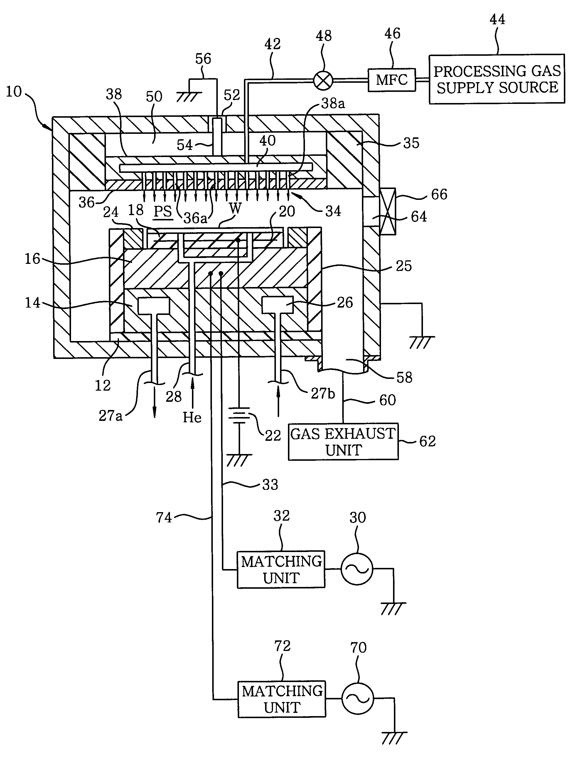
[0042]FIG. 1 illustrates a configuration of a plasma processing apparatus in accordance with the present invention. The plasma processing apparatus is configured as a capacitively coupled (parallel plate type) plasma processing apparatus of a type in which dual frequency powers are applied to a lower electrode. The plasma processing apparatus has a cylindrical vacuum chamber (processing chamber) 10 made of, e.g., an aluminum whose surface is alumite-treated (anodically oxidized), and the chamber 10 is frame grounded.

[0043]A cylindrical susceptor support 14 is provided at a bottom portion in the chamber 10 via an insulation plate 12 made of ceramic or the like. Further, a susceptor 16 made of, e.g., aluminum, is disposed above the susceptor support 14. The susceptor 16 serves as a lower electrode and a target substrate, e.g., a semiconductor wafer W, is mounted thereon.

[0044]On the top surface of the susceptor 16, there is disposed an electrostatic chuck 18 for attracting and holding...

second embodiment

[0086]In the second embodiment, the serial-parallel LC circuit 94 in the DC filter unit 82 allows the DC voltage from the variable DC power supply 84 to flow therethrough to the upper electrode 34 and generates a serial resonance at a low frequency range (preferably, from 100 kHz to 15 MHz) and a parallel resonance at a radio frequency range (preferably, from 5 MHz to 200 MHz) with respect to the radio frequency from the upper electrode 34. By utilizing such frequency-impedance characteristics of the serial-parallel LC circuit 94, it is possible to further improve the individual functions of the first and the second radio frequency in the dual frequency application type wherein two radio frequency powers are applied to the lower electrode.

[0087]FIG. 10 depicts, as an example, frequency-impedance characteristics Z94 of the serial-parallel LC circuit 94 alone in this embodiment and frequency-impedance characteristics ZA in a radio frequency transmission line from a boundary surface be...


PUM

PropertyMeasurementUnit
antiresonance frequencyaaaaaaaaaa
frequencyaaaaaaaaaa

Abstract

In a plasma processing apparatus, a first electrode is attached to a grounded evacuable processing chamber via an insulating material or a space and a second electrode disposed in parallel with the first electrode spaced apart therefrom in the processing chamber, the second electrode supporting a target substrate to face the first electrode. A first radio frequency power supply unit applies a first radio frequency power of a first frequency to the second electrode, and a second radio frequency power supply unit applies a second radio frequency power of a second frequency lower than the first frequency to the second electrode. Further, a processing gas supply unit supplies a processing gas to a processing space formed by the first and the second electrode and a sidewall of the processing chamber. Moreover, an inductor electrically is connected between the first electrode and a ground potential.

Description

FIELD OF THE INVENTION[0001]The present invention relates to a technique for performing a plasma processing on a target substrate; and, more particularly, to a capacitively coupled plasma processing apparatus of a dual frequency application mode and a plasma processing method.BACKGROUND OF THE INVENTION[0002]In a manufacturing process of semiconductor devices or flat panel displays (FPDs), a plasma is used to perform a processing, such as etching, deposition, oxidation, sputtering or the like, so as to obtain a good reaction of a processing gas at a relatively low temperature. Conventionally, a capacitively coupled type plasma apparatus has been widely employed as a single-wafer plasma processing apparatus, especially, as a single-wafer plasma etching apparatus.[0003]Generally, in the capacitively coupled plasma processing apparatus, an upper electrode and a lower electrode are disposed to face each other in parallel in a vacuum processing chamber, a substrate to be processed (a sem...

Claims


Application Information

Patent Timeline
Patent Type & Authority Applications(United States)
IPC IPC(8): B23K9/00
CPCH01J37/32165H01J37/32082
Inventor MATSUMOTO, NAOKIKOSHIMIZU, CHISHIOHAYAKAWA, YOSHINOBUHANAOKA, HIDETOSHIIWATA, MANABUTANAKA, SATOSHI
Owner TOKYO ELECTRON LTD
Why Eureka
Try Eureka