Structure of heat dissipation of implant type light emitting diode package and method for manufacturing the same

a technology of light-emitting diodes and heat-emitting diodes, which is applied in the direction of circuit thermal arrangements, printed circuit details, semiconductor devices, etc., can solve the problems of deteriorating heat produced by diodes, inability to solve heat-emitting problems, and poor overall heat-emitting effect, so as to achieve accurate heat-emitting paths, save time and labor, and produce quickly

Inactive Publication Date: 2007-10-11
EDISON-OPTO
View PDF3 Cites 37 Cited by
  • Summary
  • Abstract
  • Description
  • Claims
  • Application Information

AI Technical Summary

Benefits of technology

[0010] Therefore, the present invention is to provide a method for quickly producing a structure of heat dissipation of light emitting diode package that directly implants a heat column into a substrate, and thus the manufacture requires the manufacturing process once only and can save a great deal of time and labor. The technology of implanting the heat column can accurately establish a heat conducting path.
[0011] Another, the present invention is to provide a structure of heat dissipation of implant type light emitting diode package that directly implants a heat column into a substrate, so that the operating heat produced by the light emitting diode can be guided to the outside directly, and the light emitting power of the packaged light emitting diode will not be affected by the operating heat.

Problems solved by technology

As a result, the surrounding of the chip is the best heat dissipating are for the heat produced, but the material used for packing diodes generally adopts resins with an insulating heatproof effect, and the overall heat dissipating effect is poor.
If the entire chip and its electrode circuits are wrapped by resins, the heat cannot be dissipated successfully, which will constitute a practically heat-sealed operating environment, and the heat produced will deteriorate the diode.
However, the traditional light emitting diode package structure does not come with a heat dissipating structure for dissipating the operating heat produced by the light emitting diode, and thus some manufacturers tried to use improved package materials to conduct the operating heat produced by the light emitting diode to the outside by the high thermal conductivity of the improved material, but the materials used for the package structure still cannot solve the heat dissipating issue due to their low conductivity, or the package materials are expanded by the heat to form a gap between the light emitting diode and the package material, and thus air or moisture may enter into the diode easily and affect the operation of the diode or shorten the life of the light emitting diode.
In view of the low heat dissipating performance of the package material, some manufacturers tried to improve the heat dissipating effect by changing the materials of the circuit board, but most circuit boards are made of materials mixed with metal, fiber glass, or ceramic, and the conductivity of such materials is not consistent due to the mixed materials, and the heat dissipating effect is still limited by these materials.
The structure is manufactured by the manufacturing process technology twice, and thus the manufacture requires much time and labor.
Furthermore, the screen printing technology prints a metal paste in the penetrating hole, and thus the metal paste cannot be filled accurately into the penetrating hole and a gap may be produced to give rise to a discontinuous heat conduction.

Method used


Image

  • Structure of heat dissipation of implant type light emitting diode package and method for manufacturing the same
  • Structure of heat dissipation of implant type light emitting diode package and method for manufacturing the same
  • Structure of heat dissipation of implant type light emitting diode package and method for manufacturing the same

Examples


Embodiment Construction

[0025] The technical characteristics, features and advantages of the present invention will become apparent in the following detailed description of the preferred embodiments with reference to the accompanying drawings.

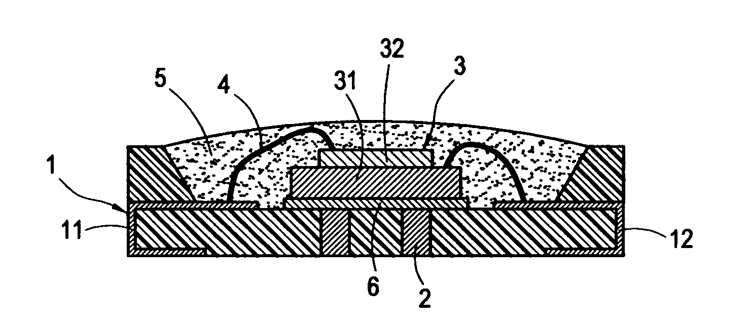
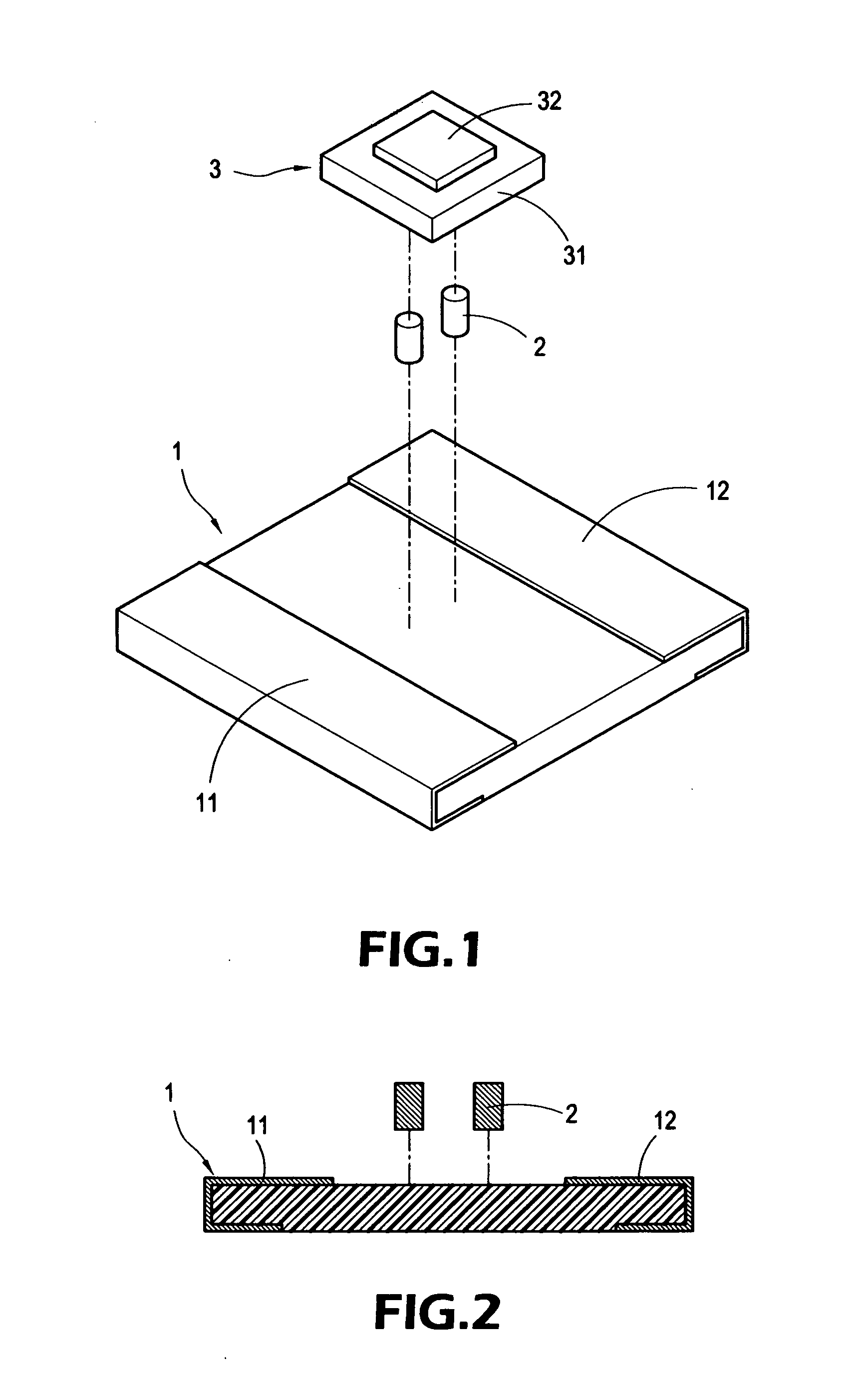
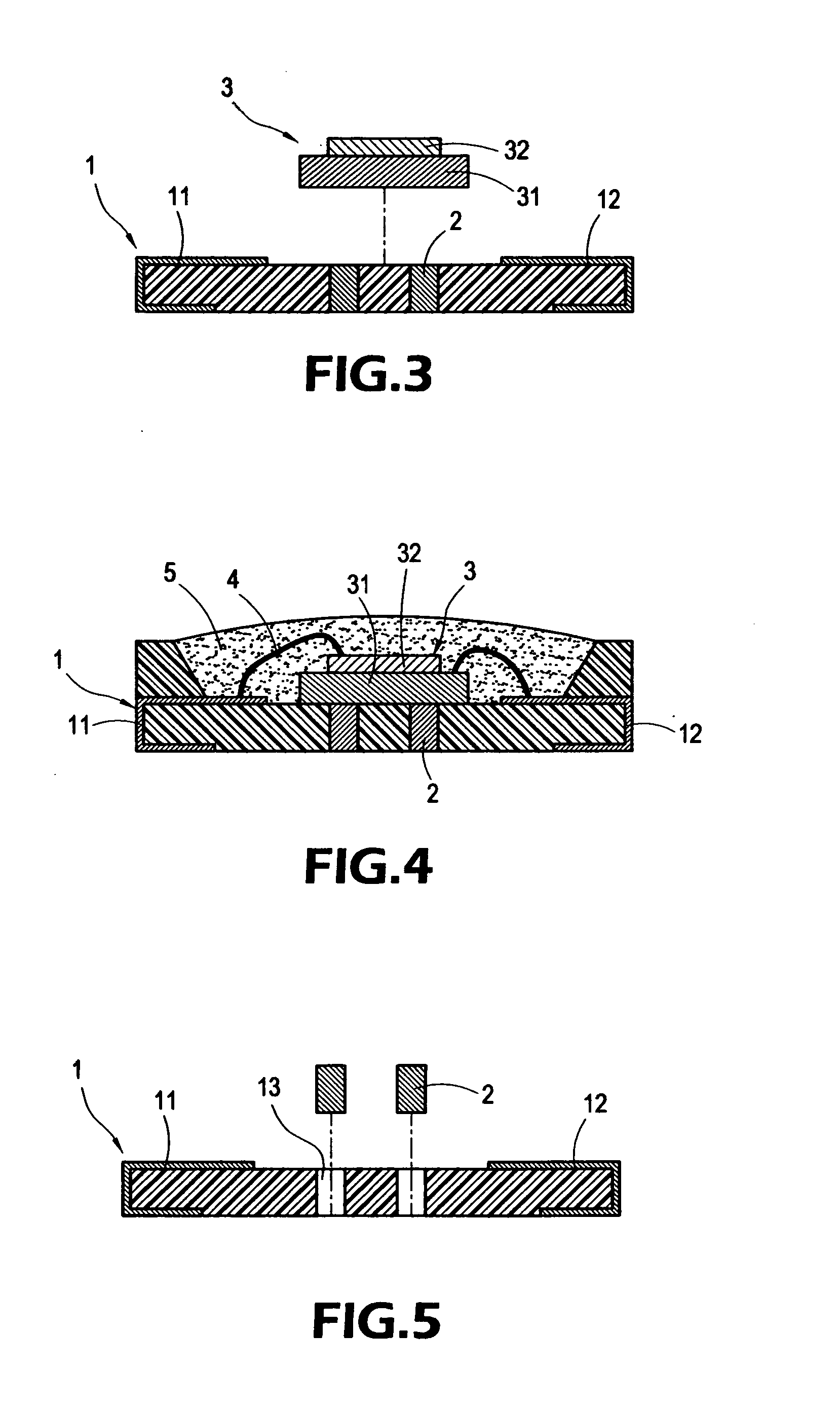
[0026] Referring to FIG. 1, a structure of the invention comprises a substrate 1, at least one heat column 2, and a light emitting diode chip 3. The substrate 1 is made of an electric insulating material, which is a printed circuit board in this preferred embodiment, and both left and right ends of the substrate 1 include a first electrode 11 and a second electrode 12 respectively to form an n-shaped structure for covering both ends of the substrate. Referring to FIG. 2, the heat column 2 is implanted directly onto a predetermined position of the light emitting diode chip 3 of the substrate 1 by a manufacturing technology such as a stamping method and penetrated through a predetermined position on both surfaces of the substrate 1. The heat column 2 is made of a highl...


PUM


Abstract

A structure of heat dissipation of implant type light emitting diode package having a heat column and a method of manufacturing the same include a substrate, a heat column, and a light emitting diode chip, and the heat column is implanted directly onto a predetermined position of the light emitting diode chip of the substrate and penetrated through both surfaces of a circuit board, and a distal surface of the heat column is coupled with the light emitting diode chip to form a heat conducting end, so that the operating heat produced by a light emitting diode can be dispersed from the package structure through the heat column, so as to achieve an optimal heat dissipating effect.

Description

BACKGROUND OF THE INVENTION [0001] 1. Field of the Invention [0002] The present invention relates to a light emitting diode, and more particular to a structure of heat dissipation of light emitting diode package and a method of manufacturing the same. [0003] 2. Description of Prior Art [0004] A light emitting diode (LED) is a solid-state semiconductor device that combines two carriers produced by passing an electric current through the LED to release energy in the form of light. LED has the advantages of a compact size, a fast response rate, and a high-performance feature, and thus the LEDs are applied extensively in different industries. Since LEDs have bottlenecks including insufficient brightness and low luminous efficiency at an early stage, a high power LED is developed later to overcome the drawback of insufficient brightness, and thus LEDs become increasingly popular in the high power illumination market and tend to gradually take over the position of traditional tungsten lam...

Claims


Application Information

Patent Timeline
Patent Type & Authority Applications(United States)
IPC IPC(8): H01L33/00H01L33/48H01L33/64
CPCH01L33/486H01L33/642H05K1/0204H01L2224/48091H01L2924/00014
Inventor SUN, TSUNG-TINGLAIO, HUNG-TAYAN, TZ-SHIUANSU, PO-JEN
Owner EDISON-OPTO
Why Eureka
Try Eureka