Wavelength converting devices

Active Publication Date: 2007-10-11
NGK INSULATORS LTD
View PDF2 Cites 13 Cited by
  • Summary
  • Abstract
  • Description
  • Claims
  • Application Information

AI Technical Summary

Benefits of technology

[0018] The inventors have variously studied the patterns of high spatial frequency in horizontal direction contained in wavelength-converted light. It was thus found that such patterns can be considerably reduced and quality of beam can be improved by covering at least a part of the back face of the additional portion with the back side metal film. The present invention is based on the discovery. However, in the case that the back face of the wavelength converting portion is covered with the back side metal film, light propagating in the wavelength converting portion would be absorbed by it to lower the output power. The back face of the wavelength converting porti

Problems solved by technology

This is due to leakage from the ridge-type optical waveguide to slab-type optical waveguides provided in both sides thereof.
Such patterns of high spatial

Method used


Image

  • Wavelength converting devices
  • Wavelength converting devices
  • Wavelength converting devices

Examples


Example

Example 1

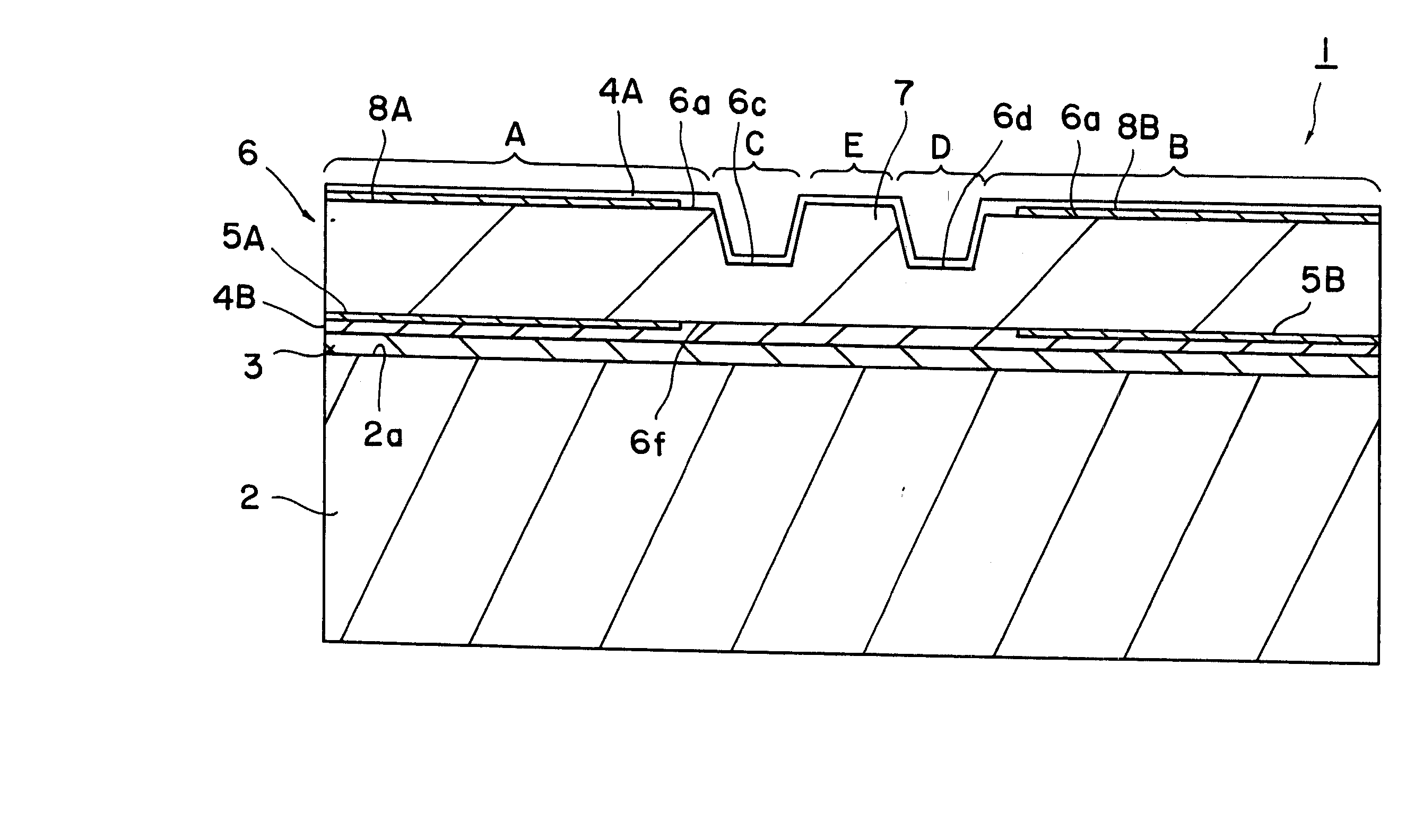
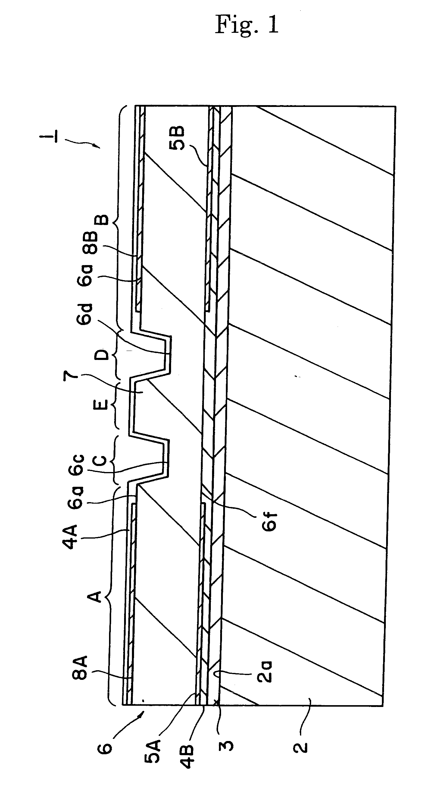
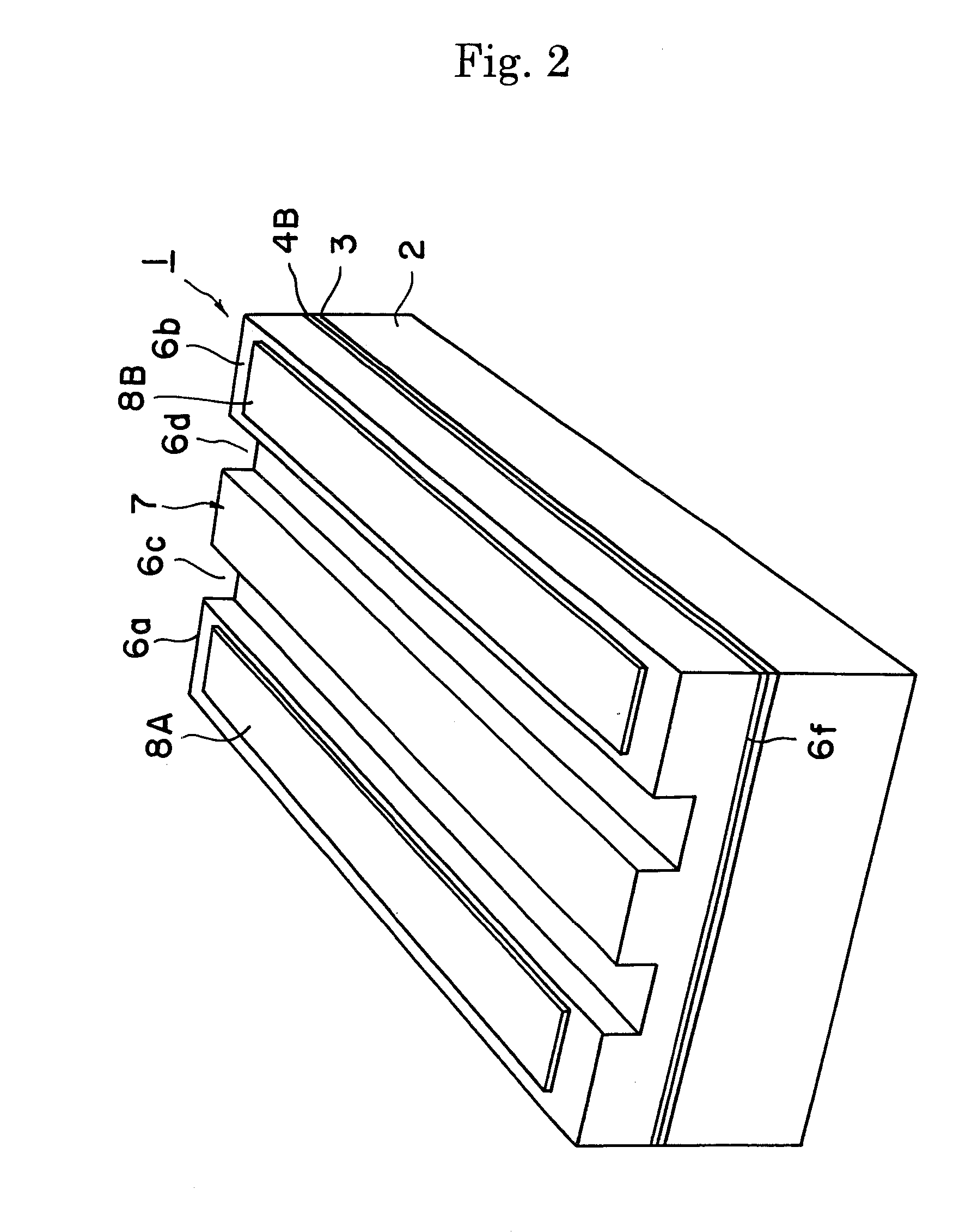
[0058] The device shown in FIG. 5 was produced. Specifically, periodic polarization domain inversion structure having a period of 6.50 μm was produced in a substrate having a thickness of 500 μm and made of MgO-doped lithium niobate. A metal film made of Al metal and having a thickness of 0.05 μm was formed thereon by sputtering. The metal film was subjected to dry etching with chlorine-series etching gas to form patterns of metal films 5A and 5B so that they are in the vicinity of the grooves for forming the optical waveguide. Thereafter, a SiO2 film 4B (buffer layer) was formed by sputtering on the whole main face of the wafer to cover the patterns of the metal films5A and 5B.

[0059] An adhesive 3 was applied onto a substrate 2 having a thickness of 1 mm and made of non-doped lithium niobate. The substrate was then adhered to the above substrate of MgO-doped lithium niobate. The surface of the substrate of MgO-doped lithium niobate was removed by grinding and polishing t...

Example

Comparative Example 1

[0061] A device was produced according to the same procedure as the Example 1, except that the back side metal films were not formed. Periodic polarization domain inversion structure having a period of 6.50 μm was produced in a substrate having a thickness of 500 μm and made of MgO-doped lithium niobate. A SiO2 film 4B (buffer layer) having a thickness of 0.5 μm was formed by sputtering. An adhesive 3 was applied onto a substrate having a thickness of 1 mm and made of non-doped lithium niobate. The substrate was then adhered to the above substrate of MgO-doped lithium niobate. The surface of the substrate of MgO-doped lithium niobate was removed by grinding and polishing to a thickness of 3.7 μm. The substrate was then processed by laser ablation to form a ridge type optical waveguide 7. The width of the ridge type optical waveguide 7 was 4.5 μm and the depth was 2 μm. After the processing of the ridge, Ta2O5 film 4A having a thickness of 0.5 μm was formed on t...

Example

Example 2

[0063] A device was produced according to the same procedure as the Example 1, except that the back side metal films were not formed and only upper side metal films 8A and 8B were provided shown in FIG. 1. The optical properties of the waveguide were measured. The SHG output power was 15 W at an input power of 100 W of the fundamental light. The quality (M2 value) of beam of SHG light was measured with a beam profiler to obtain a value of 1.2. Besides, the wavelength of the fundamental light was 1.06 μm in the optical waveguide and the wavelength of the SHG light was 0.53 μm.


PUM


Abstract

A wavelength converting device 1 has a ferroelectric layer 6 made of a ferroelectric material. The ferroelectric layer has a wavelength converting portion A having a ridge-type optical waveguide 7, additional portions A and B provided in both sides of the wavelength converting portions, respectively, and groove-forming portions C and D between the wavelength converting portion and the additional portions, respectively. The device further has a supporting body 2 adhered to a back face 6f of the ferroelectric layer 6, and back side metal films 5A and 5B covering at least a part of a back face 6f of the additional portions 6, respectively. The back side metal film 5A or 5B does not cover the back face 6f of the wavelength converting portion 6.

Description

BACKGROUND ARTS [0001] 1. Field of the Invention [0002] The invention relates to a wavelength converting device. [0003] 2. Background Arts [0004] Non-linear optical crystals, such as lithium niobate or lithium tantalite, have a high second-order non-linear optical constant. It is thus possible to realize a quasi-phase matched (QPM) type second harmonic generation (SHG) device, by providing a periodic polarization domain inversion structure in the crystal. Further, an SHG device of a high efficiency can be realized by forming a waveguide in the periodic polarization domain inversion structure. Such device finds a wide variety of applications such as optical communication, medical uses, optochemical uses, various optical measurements, etc. [0005] The applicant disclosed a process of producing a ridge-shaped optical waveguide used for a device for generating second harmonic wave, in Japanese Patent publication H09-269430A. The waveguide is formed by subjecting an oxide single crystal t...

Claims


Application Information

Patent Timeline
IPC IPC(8): G02B6/10
CPCG02F1/377G02F2201/063G02F2001/372G02F1/372
Inventor YOSHINO, TAKASHIYAMAGUCHI, SHOICHIRO
Owner NGK INSULATORS LTD
Why Eureka
Try Eureka