Manufacturing Method for a Liquid Crystal Display

a liquid crystal display and manufacturing method technology, applied in the direction of electrical equipment, semiconductor devices, instruments, etc., can solve the problems of increasing the difficulty of aligning the transistor array substrate with the color filter substrate, reducing the use of masks by the lcd manufacturer, and time-consuming steps of exposing and developing, so as to reduce the number of steps, reduce the cost of manufacturing lcd, and improve the yield rate of lcd production

Active Publication Date: 2007-10-11
AU OPTRONICS CORP
View PDF14 Cites 18 Cited by
  • Summary
  • Abstract
  • Description
  • Claims
  • Application Information

AI Technical Summary

Benefits of technology

[0009]It is therefore an objective of the present invention to provide a method for manufacturing an LCD. The method can reduce the number of steps needed for manufacturing an LCD. Therefore, the cost of manufacturing the LCD is decreased and the yield rate of the LCD production is improved, too.

Problems solved by technology

As the size of the LCD becomes increasingly larger, aligning the transistor array substrate with the color filter substrate is increasingly more difficult.
Furthermore, the LCD manufacturer takes great effort to reduce the use of masks because masks are very expensive, and steps of exposing and developing are time consuming and have many risks about aligning error.
However, the manufacturing cost and risks of the half tone masks are more than the conventional masks.

Method used


Image

  • Manufacturing Method for a Liquid Crystal Display
  • Manufacturing Method for a Liquid Crystal Display
  • Manufacturing Method for a Liquid Crystal Display

Examples


embodiment i

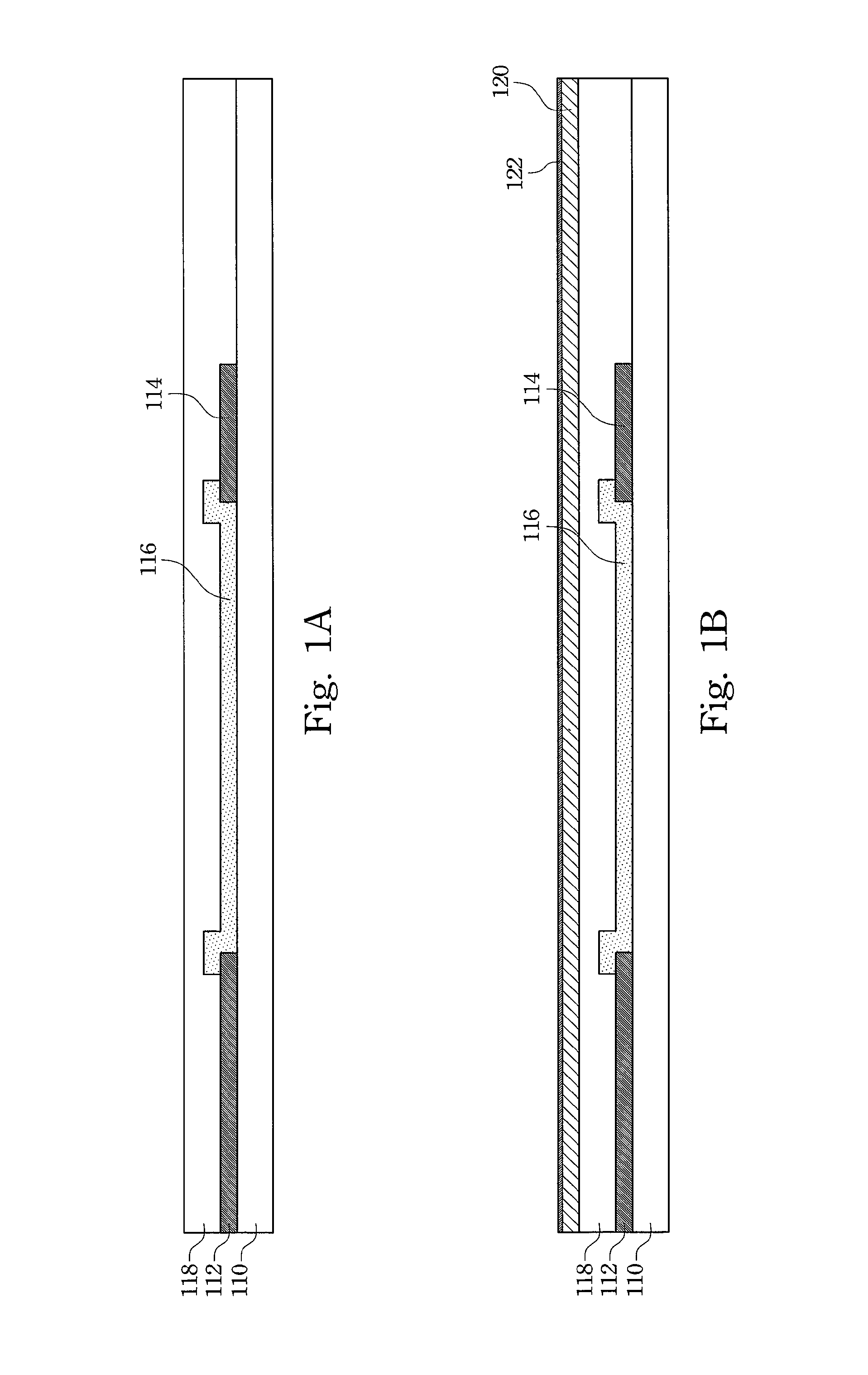
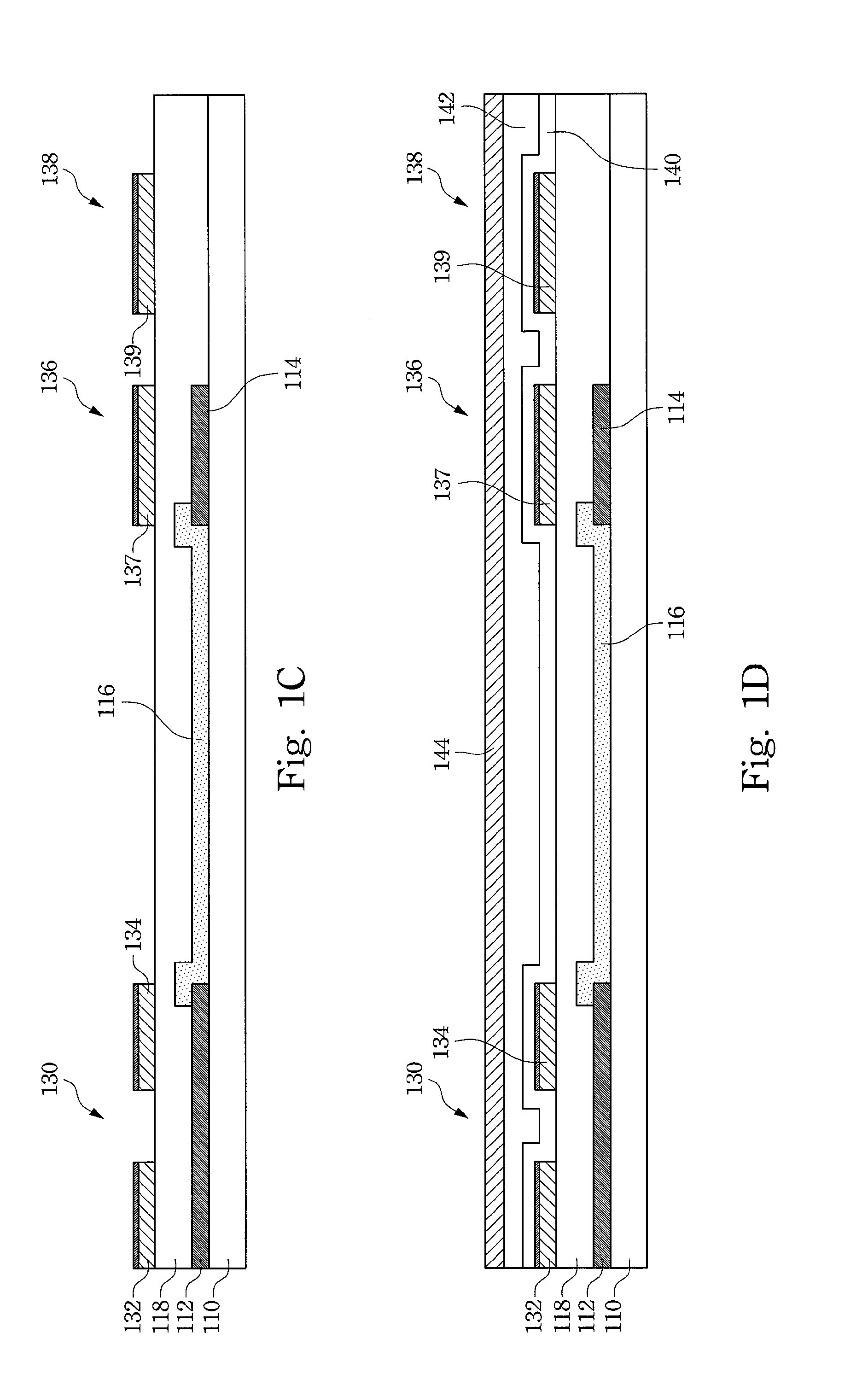
[0019]Reference is made to FIGS. 1A-1G, which are cross sectional views showing a method for manufacturing LCD according to one preferred embodiment of this invention.

[0020]In FIG. 1A, black matrices 112 / 114, a color filter layer 116 and a flatness layer 118 are formed over a transparent substrate 110 to provide a color filter substrate. The color of the color filter layer 116 may be red, blue or green. The flatness layer 118 may be a transparent organic material, such as a photo resistant material.

[0021]Referring to FIG. 1B, a first conductor layer 120 and a doped semiconductor layer 122 are formed over the flatness layer 118 in order. The material of the first conductor layer 120 may be molybdenum, chromium, iridium, aluminum, titanium, a combination thereof or an alloy thereof. The first conductor layer 120 may be formed by a physical vapor deposition process, such as sputtering. The material of the doped semiconductor layer 122 may be N type doped amorphous silicon.

[0022]In FIG....

embodiment ii

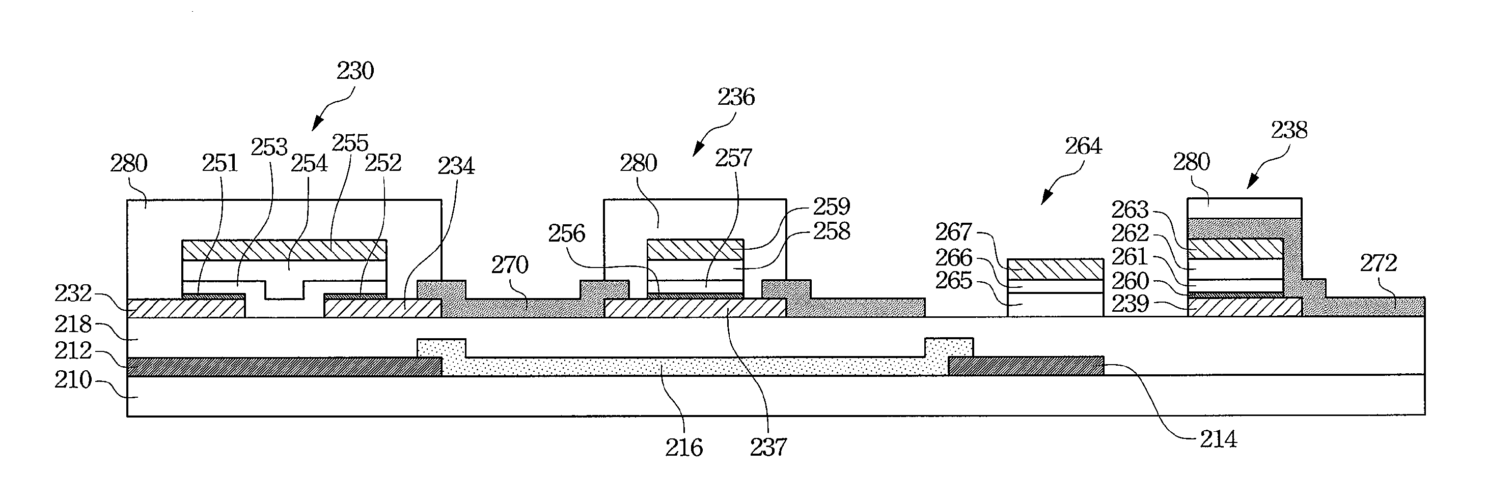
[0028]Reference is made to FIGS. 2A-2G, which are cross sectional views showing a method for manufacturing LCD according to another preferred embodiment of this invention.

[0029]In FIG. 2A, black matrices 212 / 214, a color filter layer 216 and a flatness layer 218 are formed over a transparent substrate 210 to provide a color filter substrate. The color of the color filter layer 216 may be red, blue or green. The flatness layer 218 may be a transparent organic material, such as a photo resistant material.

[0030]Referring to FIG. 2B, a first conductor layer 220 and a doped semiconductor layer 222 are formed over the flatness layer 218 in order. The material of the first conductor layer 220 may be molybdenum, chromium, iridium, aluminum, titanium, a combination thereof or an alloy thereof. The first conductor layer 220 may be formed by a physical vapor deposition process, such as sputtering. The material of the doped semiconductor layer 222 may be N type doped amorphous silicon.

[0031]In ...


PUM


Abstract

A method for manufacturing a liquid crystal display includes the following steps. First, source/drain and a bottom electrode are formed over a color filter substrate with a color filter layer. The next step forms source/drain junction regions over the source/drain. A channel region is also formed between the source/drain in this step. A gate dielectric layer and a gate are formed over the channel region and the source/drain junction regions in this step as well. Moreover, a plurality of stack layers and an upper electrode are formed over the bottom electrode in this step, too. Then, a pixel electrode is formed to electrically connect one of the source/drain and the bottom electrode. Then, a passivation layer pattern is formed to cover the source/drain, the gate, the upper electrode and the bottom electrode by backside exposure. Finally, a plurality of steps are performed to finish the liquid crystal display.

Description

RELATED APPLICATIONS[0001]The present application is based on, and claims priority from, Taiwan Application Serial Number 95112880, filed Apr. 11, 2006, the disclosure of which is hereby incorporated by reference herein in its entirety.BACKGROUND[0002]1. Field of Invention[0003]The present invention relates to a liquid crystal display. More particularly, the present invention relates to a method for forming thin film transistor arrays on a color filter.[0004]2. Description of Related Art[0005]Liquid crystal displays (LCD) have been widely applied in electrical products because of their high image quality, compact size, light weight, low driving voltage and low power consumption. LCDs have been introduced into portable computers, personal digital assistants and color televisions and are becoming the mainstream display apparatus.[0006]A conventional LCD includes a transistor array substrate, a color filter substrate and liquid crystals filled between the transistor array substrate and...

Claims


Application Information

Patent Timeline
Patent Type & Authority Applications(United States)
IPC IPC(8): H01L21/00
CPCG02F2001/136222G02F1/136209G02F1/136222G02F1/136
Inventor SHIH, MING-HUNG
Owner AU OPTRONICS CORP
Why Eureka
Try Eureka