Semiconductor transistors having reduced channel widths and methods of fabricating same

a technology of semiconductor transistors and channel widths, which is applied in the direction of semiconductor devices, basic electric elements, electrical equipment, etc., can solve the problems of limiting the manufacturability of the channel, higher on-state resistance of the device, and higher power dissipation

Active Publication Date: 2007-10-11
GENERAL ELECTRIC CO
View PDF9 Cites 119 Cited by
  • Summary
  • Abstract
  • Description
  • Claims
  • Application Information

AI Technical Summary

Benefits of technology

[0009] In one embodiment of the invention, a semiconductor device having at least one semiconductor layer and a patterned masking layer over the at least one semiconductor layer is provided. The patterned masking layer has an opening therethrough wherein the opening has a first width. The device further includes a screening layer over the at least one semiconductor layer and the patterned masking layer wherein the screening layer is in a range of about 100 Å to about 7000 Å.

Problems solved by technology

Disadvantageously, relying on the alignment of multiple lithography steps to form the channel of a power MOSFET limits the manufacturability of

Method used


Image

  • Semiconductor transistors having reduced channel widths and methods of fabricating same
  • Semiconductor transistors having reduced channel widths and methods of fabricating same
  • Semiconductor transistors having reduced channel widths and methods of fabricating same

Examples


Embodiment Construction

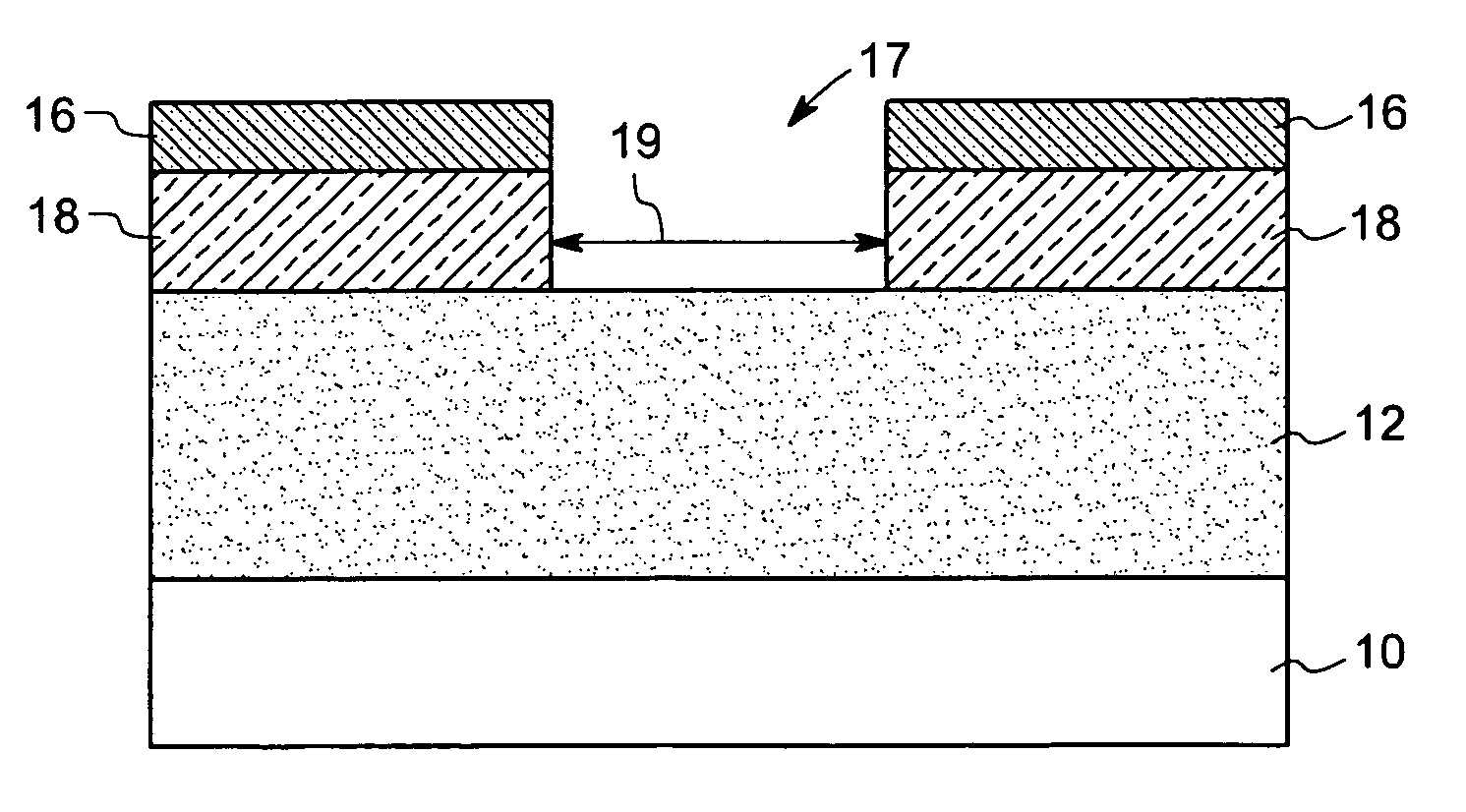
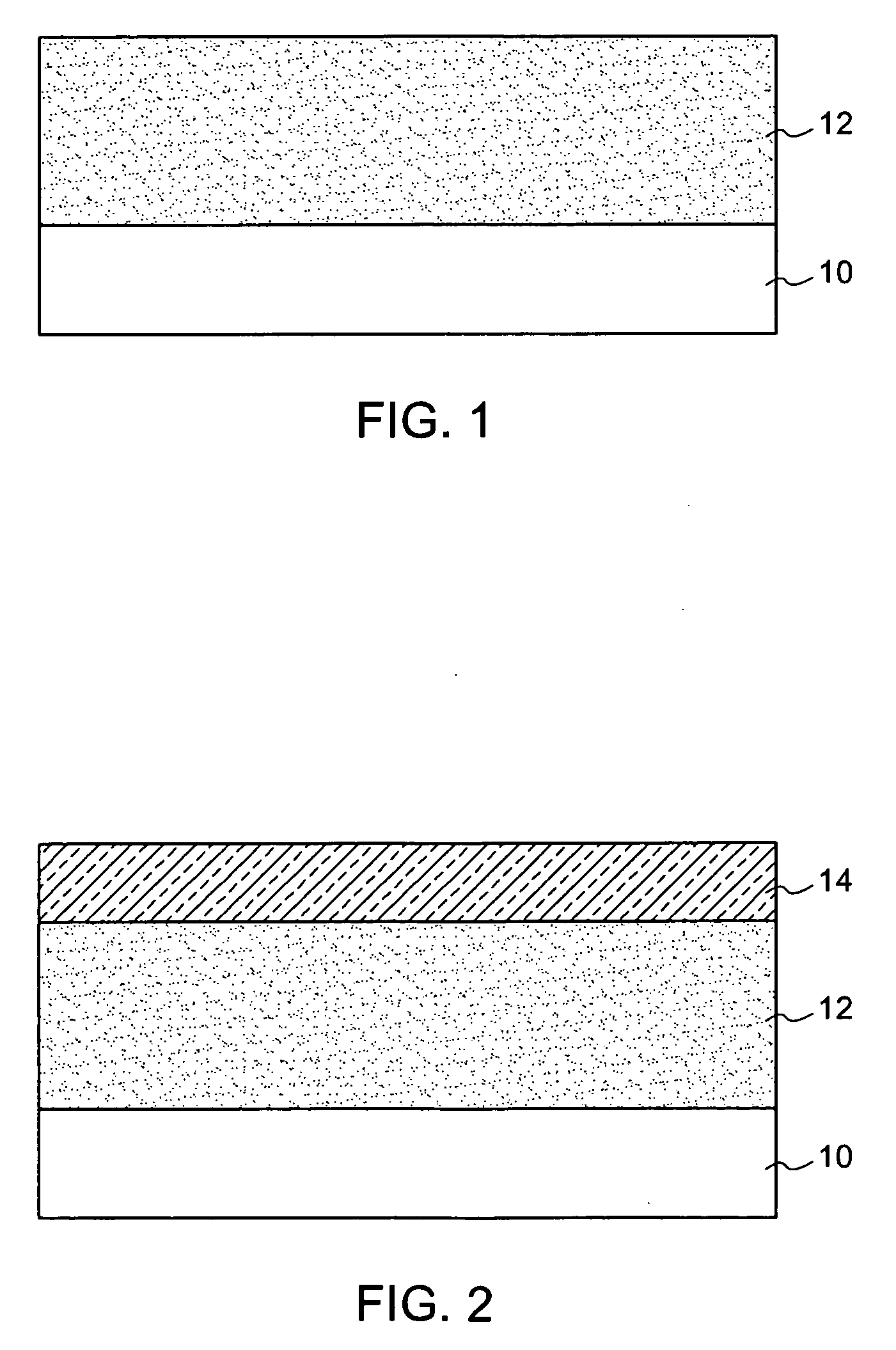
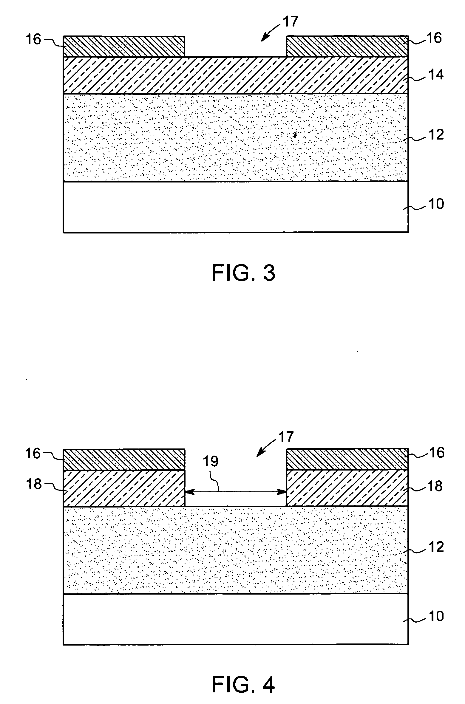
[0015] A typical metal oxide field effect transistor (MOSFET) includes a source region, a drain region and a gate. Similarly, the related insulated gate bipolar transistor (IGBT) includes an emitter, a collector and a base, respectively, corresponding to the components of a MOSFET. In these devices, the source region or the drain region, and the emitter or the collector, are differently doped than an underlying semiconductor layer / substrate. In other words, if the source region is doped with n-type dopants then the underlying semiconductor layer is doped with p-type dopants. Typically, the doping may be performed through multiple lithography steps including a diffusion process whereby the respective dopants are diffused in the semiconductor layer / substrate selectively by making use of more than one masking layer. As the diffusion coefficients of the dopants in silicon carbide (SiC) are negligible, diffusion may not be a viable option for fabrication of devices based on silicon carbi...


PUM


Abstract

A method of forming a channel in a semiconductor device including forming an opening in a masking layer to expose a portion of an underlying semiconductor layer through the opening is provided. The method further includes disposing a screening layer and implanting a first type of ions in the portion of the underlying semiconductor layer through the screening layer and through the opening in the masking layer. A second type of ions are implanted in the portion of the underlying semiconductor layer through the screening layer and through the opening in the masking layer at an oblique ion implantation angle wherein a lateral spread of second type ions is greater than a lateral spread of first type ions. Semiconductor devices fabricated in accordance to above said method is also provided.

Description

BACKGROUND [0001] The invention relates generally to semiconductor devices and in particular to semiconductor transistor devices having reduced channel widths and methods of fabricating same. [0002] As will be appreciated, transistors, such as MOSFETs (metal oxide field effect transistors), generally include a number of layers wherein many doped regions are formed. Unlike silicon-based devices, wherein doped regions are typically formed by diffusion, the doped regions in silicon carbide (SiC) based devices are generally formed through ion implantation. Thus, for certain devices, such as SiC-based devices, the formation of the various doped regions is achieved through ion implantation which may be conducted through one or more openings formed through a series of lithography steps. [0003] For instance, for a power MOSFET device, the channel formation typically involves the deposition and patterning of at least two photolithographic layers. Specifically, in conventional techniques, a P...

Claims


Application Information

Patent Timeline
IPC IPC(8): H01L21/336
CPCH01L21/046H01L29/7827H01L29/66068
Inventor TUCKER, JESSE BERKLEY
Owner GENERAL ELECTRIC CO
Why Eureka
Try Eureka