Epitaxial growth of compound nitride semiconductor structures

a compound nitride and semiconductor technology, applied in the direction of polycrystalline material growth, instruments, under a protective fluid, etc., can solve the problems of poor luminescence of devices, impede the practical fabrication of such devices, and difficulty in efficient p-doping of such materials, so as to enhance the uniformity of deposited materials and accelerate growth

Inactive Publication Date: 2007-10-18
APPLIED MATERIALS INC
View PDF102 Cites 97 Cited by
  • Summary
  • Abstract
  • Description
  • Claims
  • Application Information

AI Technical Summary

Benefits of technology

[0008] A transition layer may sometimes be deposited on the first layer in the second processing chamber before depositing the second layer. The transition layer has a chemical composition substantially the same as the first layer and a thickness less than 10,0000 Å. The first proc

Problems solved by technology

While some modestly successful efforts had previously been made in the production of blue LEDs using SiC materials, such devices suffered from poor luminescence as a consequence of the fact that their electronic structure has an indirect bandgap.
While the feasibility of using GaN to create photoluminescence in the blue region of the spectrum has been known for decades, there were numerous barriers that impeded their practical fabrication.
These included the lack of a suitable substrate on which to grow the GaN structures, generally high thermal requirements for growing GaN that resulted in various the

Method used


Image

  • Epitaxial growth of compound nitride semiconductor structures
  • Epitaxial growth of compound nitride semiconductor structures
  • Epitaxial growth of compound nitride semiconductor structures

Examples


Embodiment Construction

1. Overview

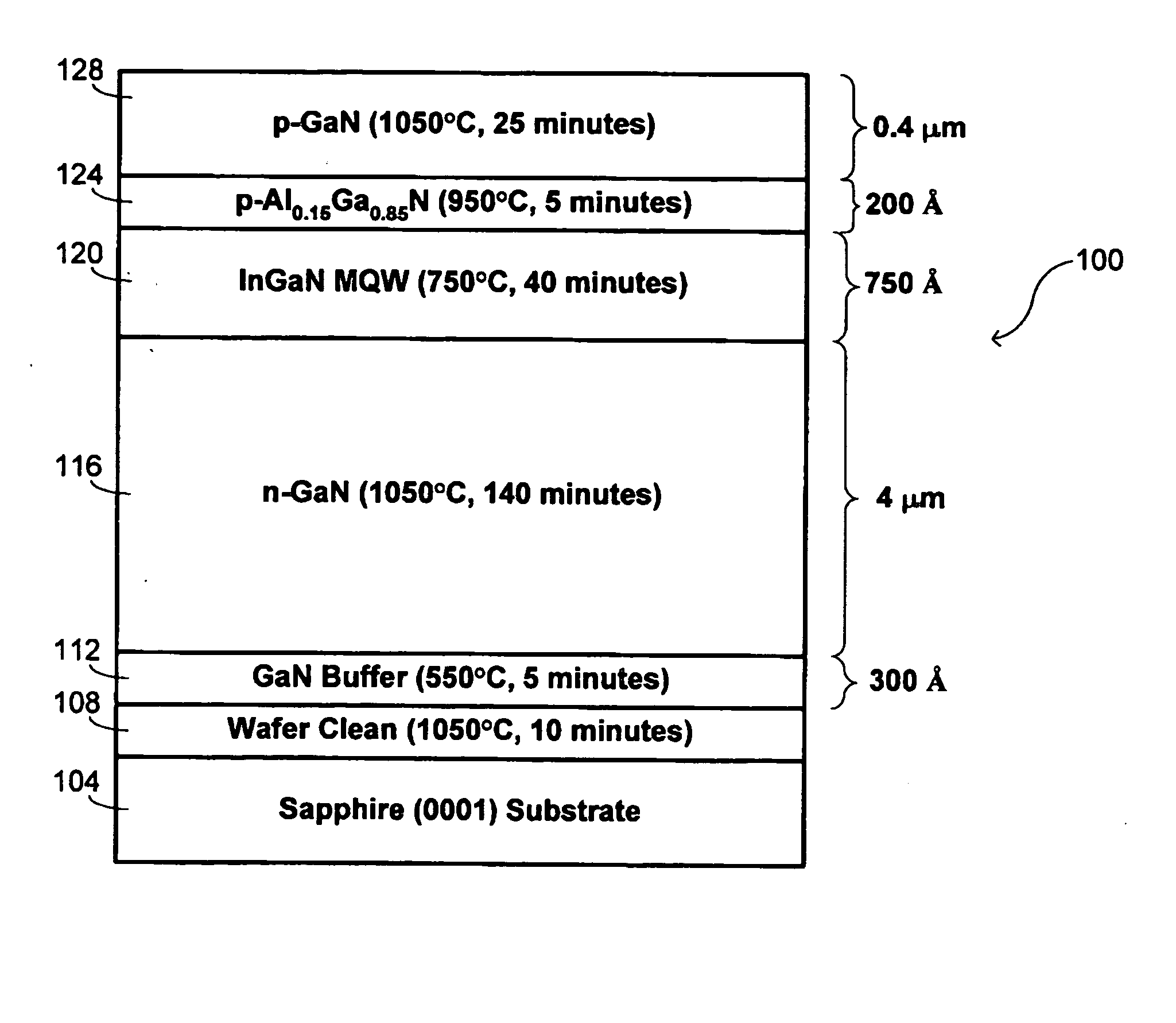
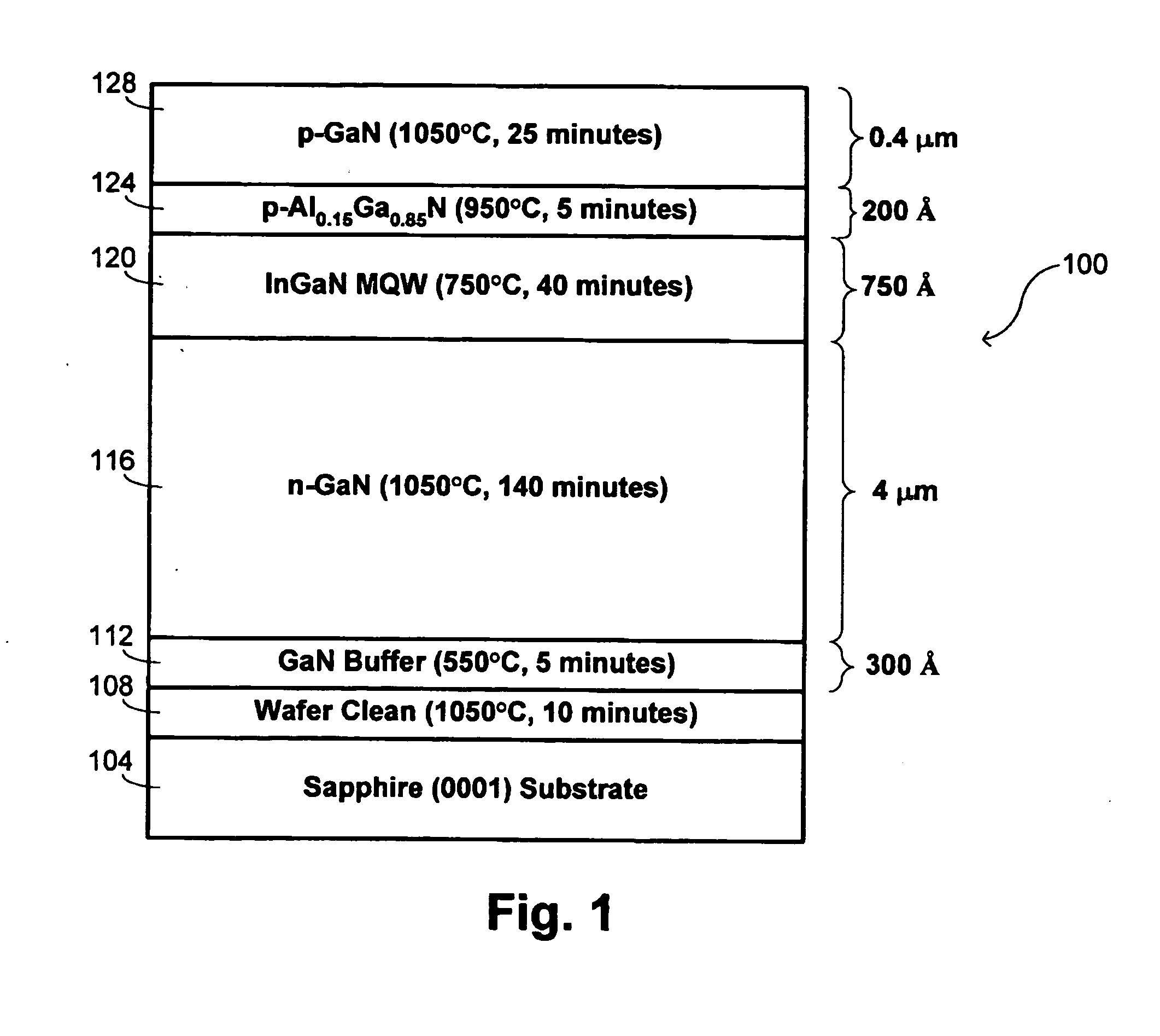
[0018] In conventional manufacturing of compound nitride semiconductor structures, multiple epitaxial deposition steps are performed in a single process reactor, with the substrate not leaving the reactor until all of the steps have been completed. The illustration in FIG. 1 shows both the types of structures that may be formed and the sequence of steps used in fabricating such a structure. In this instance, the structure is a Ga—N-based LED structure 100. It is fabricated over a sapphire (0001) substrate 104, which is subjected to a wafer cleaning procedure 108. A suitable clean time is 10 minutes at 1050° C., which may be accompanied by additional time on the order of 10 minutes for heat-up and cool-down.

[0019] A GaN buffer layer 112 is deposited over the cleaned substrate 104 using a metalorganic chemical-vapor-deposition (“MOCVD”) process. This may be accomplished by providing flows of Ga and N precursors to the reactor and using thermal processes to achieve deposit...


PUM


Abstract

Apparatus and methods are described for fabricating a compound nitride semiconductor structure. Group-III and nitrogen precursors are flowed into a first processing chamber to deposit a first layer over a substrate with a thermal chemical-vapor-deposition process. The substrate is transferred from the first processing chamber to a second processing chamber. Group-III and nitrogen precursors are flowed into the second processing chamber to deposit a second layer over the first layer with a thermal chemical-vapor-deposition process. The first and second group-III precursors have different group-III elements.

Description

BACKGROUND OF THE INVENTION [0001] The history of light-emitting diodes (“LEDs”) is sometimes characterized as a “crawl up the spectrum.” This is because the first commercial LEDs produced light in the infrared portion of the spectrum, followed by the development of red LEDs that used GaAsP on a GaAs substrate. This was, in turn, followed by the use of GaP LEDs with improved efficiency that permitted the production of both brighter red LEDs and orange LEDs. Refinements in the use of GaP then permitted the development of green LEDs, with dual GaP chips (one in red and one in green) permitting the generation of yellow light. Further improvements in efficiency in this portion of the spectrum were later enabled through the use of GaAlAsP and InGaAlP materials. [0002] This evolution towards the production of LEDs that provide light at progressively shorter wavelengths has generally been desirable not only for its ability to provide broad spectral coverage but because diode production of ...

Claims


Application Information

Patent Timeline
IPC IPC(8): C30B15/00C30B23/00G06F7/00C30B28/14
CPCC30B25/14C30B29/403C30B35/00H01L21/67155H01L21/02458H01L21/0254H01L21/0262H01L21/0242
Inventor NIJHAWAN, SANDEEPBOUR, DAVIDWASHINGTON, LORISMITH, JACOBSTEVENS, RONALDEAGLESHAM, DAVID
Owner APPLIED MATERIALS INC
Why Eureka
Try Eureka