Semiconductor memory device and manufacturing method thereof

a technology of semiconductor memory and semiconductor layers, applied in semiconductor devices, solid-state devices, decorative arts, etc., can solve the problems of heat is liable to dissipate upwards, and the thickness of the film becomes too thin, so as to reduce the electric current required for causing the phase-change and prevent the peeling of the phase-change layer. , the effect of forming stably

Active Publication Date: 2007-10-25
MICRON TECH INC
View PDF2 Cites 25 Cited by
  • Summary
  • Abstract
  • Description
  • Claims
  • Application Information

AI Technical Summary

Benefits of technology

[0016]It is therefore an object of the present invention to provide a semiconductor memory device which ensures stable formation of a phase-change layer, and is capable of reducing the current required to cause the phase change of the phase-change layer.
[0017]It is also an object of the present invention to provide a semiconductor memory device capable of efficiently heating the phase-change layer.
[0025]According to the present invention, the phase-change layer is provided with a tapered portion, whereby the contact region between the phase-change layer and lower electrode can be restricted without using an oxide film. Accordingly, the phase-change layer can be formed on a flat surface, and hence can be formed stably in a uniform thickness. This prevents the peel-off of the phase-change layer.
[0026]Further, according to the present invention, the tapered portion of the phase-change layer is provided above the region where the phase-change layer is in contact with the lower electrode. This restricts the region where the phase change is caused to occur by heating with the use of the lower and upper electrodes, and thus the electric current required for causing the phase-change can be reduced.
[0027]According to the present invention, the tapered portion is filled with an oxide film, whereby the prevention of peel-off of the phase-change layer is improved and the heat dissipation can be suppressed effectively.
[0028]Still further, according to the present invention, the lower electrode layer is formed into a shape defined by cutting off a part of the cup shape of the lower electrode in correspondence with the shape of the tapered portion of the phase-change layer. This makes it possible to suppress the heat dissipation from the lower electrode and to heat the phase-change layer even more efficiently.

Problems solved by technology

This may induce a problem that the film thickness becomes too thin in a step portion of the patterned oxide film, or a gap is formed between the phase-change layer and the oxide film or the lower electrode.
Formation of a gap may lead to peel-off of the phase-change layer.
Therefore, there is nothing to restrict heat transfer above the phase-change layer, and heat is liable to dissipate upwards.
This means that the lower electrode has a large surface area, and the heat from the phase-change layer is liable to be dissipated due to heat discharge from the lower electrode.

Method used


Image

  • Semiconductor memory device and manufacturing method thereof
  • Semiconductor memory device and manufacturing method thereof
  • Semiconductor memory device and manufacturing method thereof

Examples


Embodiment Construction

[0034]Preferred embodiments of the present invention will be described with reference to the accompanying drawings.

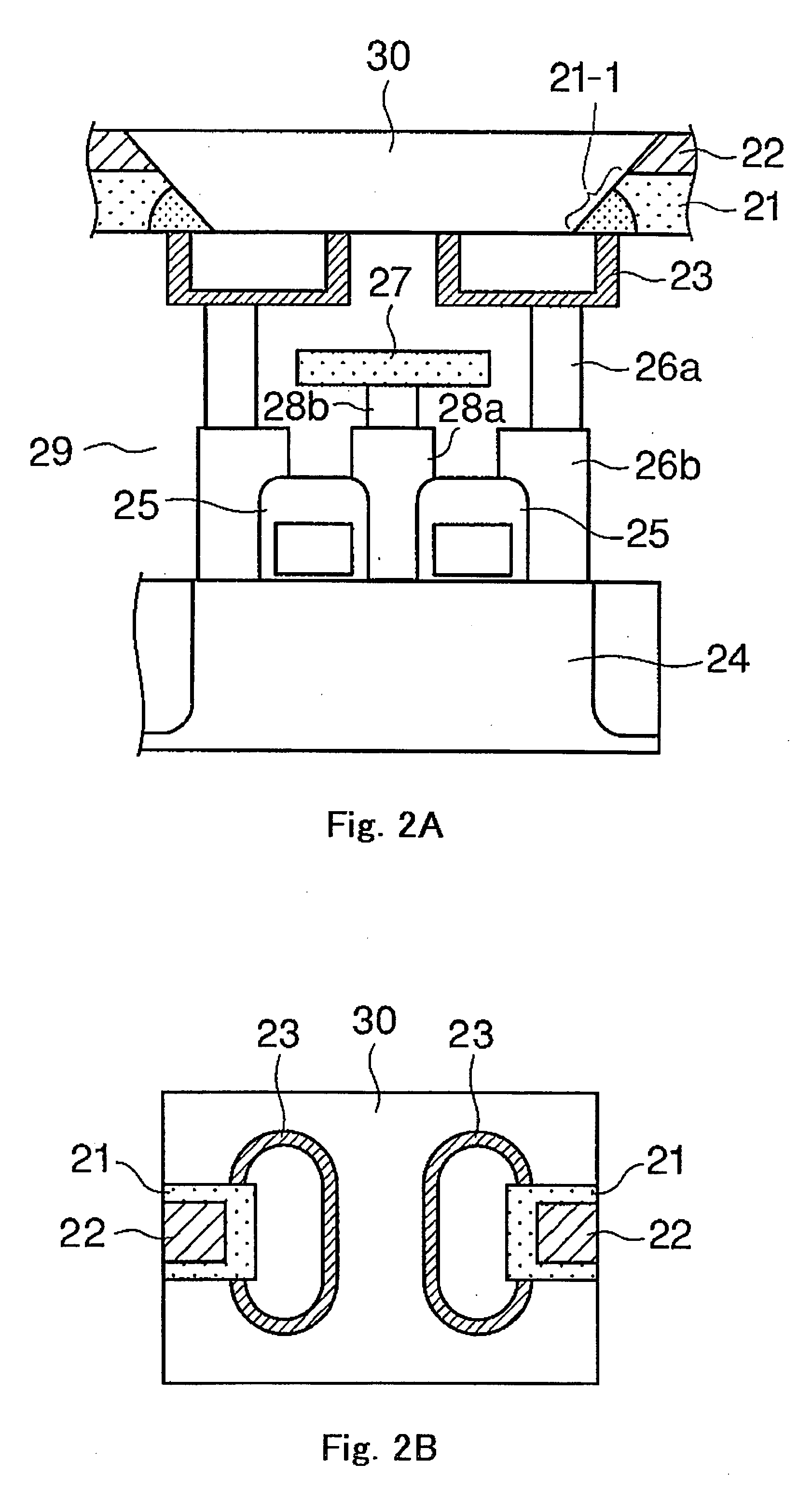
[0035]FIG. 2A is a sectional view and FIG. 2B is a plan view of a semiconductor memory device according to an embodiment of the present invention.

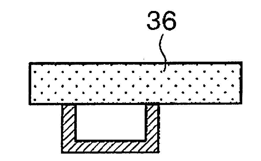
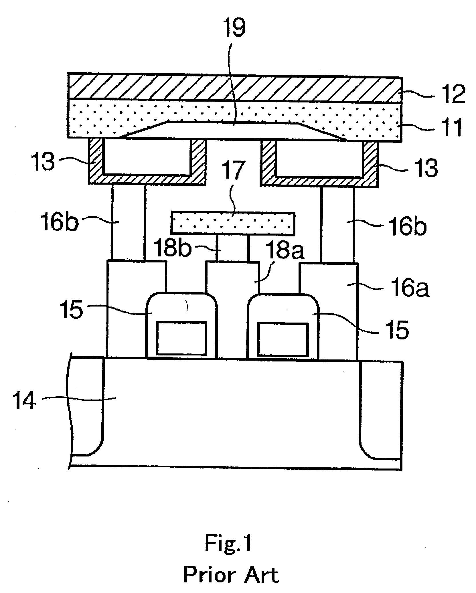
[0036]As shown FIG. 2A, the semiconductor memory device according to this embodiment has a phase-change layer 21 formed of a film of a chalcogenide (GST) as a phase change material, and upper electrodes 22 and lower electrodes 23 for heating the phase-change layer 21 by supplying electric current through the phase-change layer 21.

[0037]The semiconductor memory device further has transistors (not shown) formed in a substrate 24 in a diffused manner for controlling the supply of current to the lower electrodes 23, gate electrodes 25 connected to gates of the transistors, series of contacts 26a and 26b for connecting drains of the transistors to the lower electrodes 23, a ground wiring 27, and a series of contacts 28a and 28b for...


PUM

PropertyMeasurementUnit
areaaaaaaaaaaa
shapeaaaaaaaaaa
electric resistanceaaaaaaaaaa

Abstract

A semiconductor memory device is provided in which a phase-change layer can be formed stably and electric current required to cause the phase change of the phase-change layer can be reduced. An edge portion of the phase-change layer is formed above a lower electrode. The edge portion is formed to assume a tapered shape in cross section such that the thickness of the phase-change layer varies above the contact area between the lower electrode and the phase-change layer. The tapered portion is filled with an oxide film. According to this configuration, the region in which the phase-change occurs can be restricted, and hence the phase-change layer can be heated efficiently, resulting in reduction of electric current required for heating.

Description

[0001]This application claims priority to prior Japanese application JP 2006-116388, the disclosure of which is incorporated herein by reference.BACKGROUND OF THE INVENTION[0002]The present invention relates to a semiconductor memory device, in particular to a semiconductor memory device referred to as a phase-change type memory and a manufacturing method thereof.[0003]Recently, a phase-change random access memory (PRAM) has been proposed as a semiconductor memory an alternative to DRAM. The PRAM uses a phase change material for a recording layer to record information.[0004]The phase change material is able to freely transit between a crystal state and an amorphous state according to heat conditions. The phase change material has an electric resistance value in the crystal state that is significantly different from that in the amorphous state. Utilizing such properties of the phase change material, the PRAM stores data by changing the phase state of the phase change material accordi...

Claims


Application Information

Patent Timeline
Patent Type & Authority Applications(United States)
IPC IPC(8): C23F1/00C03C25/68
CPCH01L27/2436H01L45/06H01L45/122H01L45/1675H01L45/143H01L45/144H01L45/148H01L45/126H10B63/30H10N70/231H10N70/821H10N70/8413H10N70/8825H10N70/8828H10N70/884H10N70/063
Inventor SATO, HOMARE
Owner MICRON TECH INC
Why Eureka
Try Eureka