Light emitting device

a technology of light-emitting devices and light-emitting tubes, which is applied in the direction of display means, transportation and packaging, lighting and heating apparatus, etc., can solve the problems of low yield and achieve the effects of preventing the cracking and bending of packages due to low package strength, good mechanical strength, and preventing deformation caused by thermal expansion

Active Publication Date: 2007-10-25
NICHIA CORP
View PDF3 Cites 30 Cited by
  • Summary
  • Abstract
  • Description
  • Claims
  • Application Information

AI Technical Summary

Benefits of technology

[0010]The present invention was conceived in an effort to solve these problems, and it is an object thereof to provide a light emitting device with which adequate package strength can be ensured, handling and yield are improved, the thinner and more compact size desired in the past can be achieved by utilizing the space inside the light emitting device more efficiently, and the mounting space accounted for by the device can be kept to a minimum.
[0018]With the light emitting device of the present invention, the chipping and bending of a package due to low package strength are prevented, and deformation caused by thermal expansion is also prevented, which ensures good mechanical strength and improves handling and yield. Also, the thinner and more compact size desired in the past can be achieved by utilizing the space inside the light emitting device more efficiently, and the mounting space accounted for by the device can be kept to a minimum.
[0019]Furthermore, even when a package is produced by a conventional method such as injection molding or compression molding, for example, the occurrence of “short shot” can be prevented, and the package material can be prevented from leaking out from the lead frame portions, which makes manufacture easier and allows a light emitting device of higher quality to be obtained.

Problems solved by technology

However, if the package itself is made thinner, the low strength of the package may cause it to bend or chip, and this lowers the yield.

Method used


Image

  • Light emitting device
  • Light emitting device
  • Light emitting device

Examples


example 1

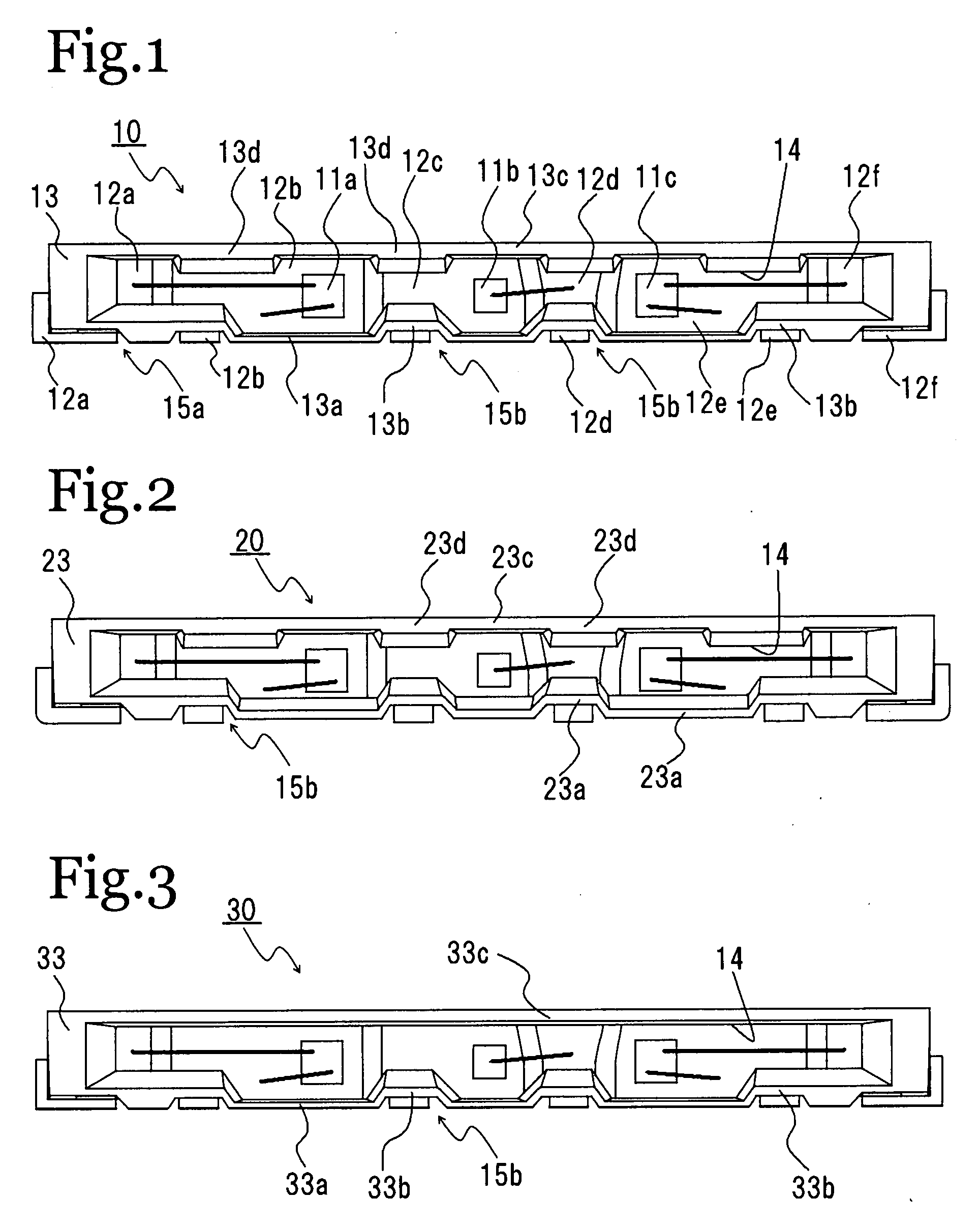
[0054]As shown in FIG. 1, the light emitting device 10 in this example comprises three light emitting elements 11a, 11b, and 11c corresponding to RGB, lead frames 12b, 12c, and 12e on which these light emitting elements are mounted and which are electrically connected by wires to one of the electrodes of the light emitting elements, three lead frames 12a, 12d, and 12f that are electrically connected by wires to the other electrode of these light emitting elements, and a package 13 that integrally fixes the lead frames 12a to 12f.

[0055]The lead frames 12a to 12f are formed as flat pieces composed of an iron alloy of copper. The lead frames 12a to 12f each comprise a region in which a light emitting element is located, or which is electrically connected to a light emitting element, and a portion that protrudes from this region to the outside of the package and functions as a lead terminal. The lead frames 12a to 12f functioning as lead terminals are portions on the exterior of the pa...

example 2

[0063]As shown in FIG. 2, the light emitting device 20 in this example is constituted substantially the same as the light emitting device in Example 1, except that near the concave portion 15b corresponding to the portion where the lead frames 12a to 12f protrude, the wall 23a of the package 23 is formed in a constant thickness and so that the taper angle is also substantially the same, and the thicker portion 23d and the thinner portion 23c are formed only on the side from which the lead frames 12a to 12f do not protrude.

[0064]This light emitting device can have enough mechanical strength while taking up the minimum amount of space, and can be easily mounted on a circuit board. Furthermore the space required for mounting on a circuit board can be kept to a minimum, which affords greater latitude in combining it with other electronic devices. In addition, other electronic devices can be disposed closer to the light emitting device, so the size and weight of a device can be reduced w...

example 3

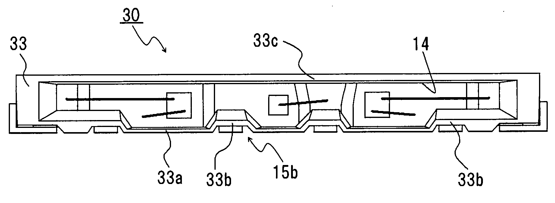
[0065]As shown in FIG. 3, the light emitting device 30 in this example is constituted substantially the same as the light emitting device in Example 1, except that the wall 33c on the side of the package 33 from which the lead frames 12a to 12f do not protrude is formed in a constant thickness, and the thicker portion 33b is formed near the concave portion 15b corresponding to the portion where the lead frames 12a to 12f protrude, while the thinner portion 33a is formed in all other portions.

[0066]The same effect can be obtained with this light emitting device as with Example 1.


PUM


Abstract

A light emitting device comprises: a light emitting element; a plurality of lead frames to which the light emitting element is electrically connected; and a package that includes in its interior at least part of said lead frames which protrude outward at one end, that is equipped with an opening for taking off light from the light emitting element, and that extends in the lengthwise direction, wherein a concave portion is formed in the outer surface of at least part of the package wall, the lead frames protruding outward from the package are accommodated in this concave portion, and the walls that constitute said opening and are across from each other in the widthwise direction of the package comprise at least a first wall that is across from the light emitting element, a second wall that is raised up by a step from the first wall, and a third wall that links the first wall and the second wall, and the second wall and third wall are formed thicker than the first wall.

Description

BACKGROUND OF THE INVENTION[0001]1. Field of the Invention[0002]The present invention relates to a light emitting device, and more particularly relates to a surface mount type of light emitting device that is compact and lightweight.[0003]2. Background Information[0004]Light emitting devices that are compact, have good sensitivity, and have light emitting elements with high brightness and high output have been developed and put to use in various fields in recent years. Because of their compact size, low power consumption, light weight, and other advantages, such light emitting devices have been used, for example, for light sources in portable telephones and liquid crystal backlights, as light sources for various kinds of meter, and as various kinds of read-out sensor.[0005]A light source used for a backlight, for example, needs to have a thin construction so that the device in which it is used can be made more compact and lightweight. Therefore, the light emitting device used as the...

Claims


Application Information

Patent Timeline
Patent Type & Authority Applications(United States)
IPC IPC(8): F21V15/01F21V9/00H01L33/56H01L33/60H01L33/62
CPCH01L25/0753H01L33/486H01L33/60Y10S362/80H01L2224/48247H01L2224/48465H01L2924/01322H01L2924/00H01L33/48H01L33/54H01L33/62
Inventor KONO, HIROSHIISHIDA, MASASHIYAMAMOTO, SAIKI
Owner NICHIA CORP
Why Eureka
Try Eureka