

Shift register circuit and image display comprising the same
a technology of shift register and image display, which is applied in the direction of logic circuits, digital storage, instruments, etc., can solve the problems of reducing the rising and falling speed of output signals, affecting the operation of unit shift registers, and affecting the implementation of high-speed operations. , to achieve the effect of preventing the reduction of drive capability and preventing the reduction of defective operations
- Summary
- Abstract
- Description
- Claims
- Application Information
AI Technical Summary
Benefits of technology
Problems solved by technology
Method used
Image

Examples
embodiment 1
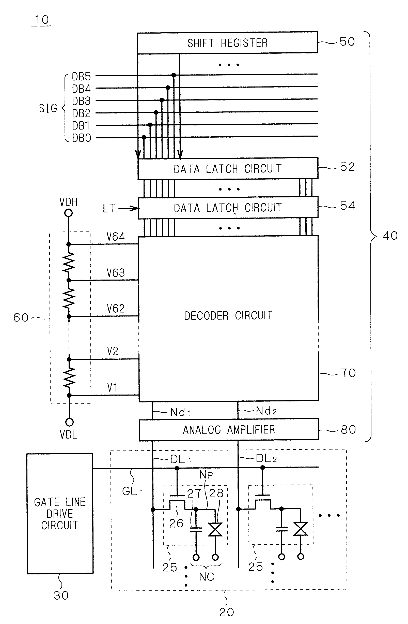
[0057]FIG. 1 is a schematic block diagram showing the constitution of a display according to an embodiment 1 of the present invention and showing the whole constitution of a liquid crystal display 10 as a representative example of the display.
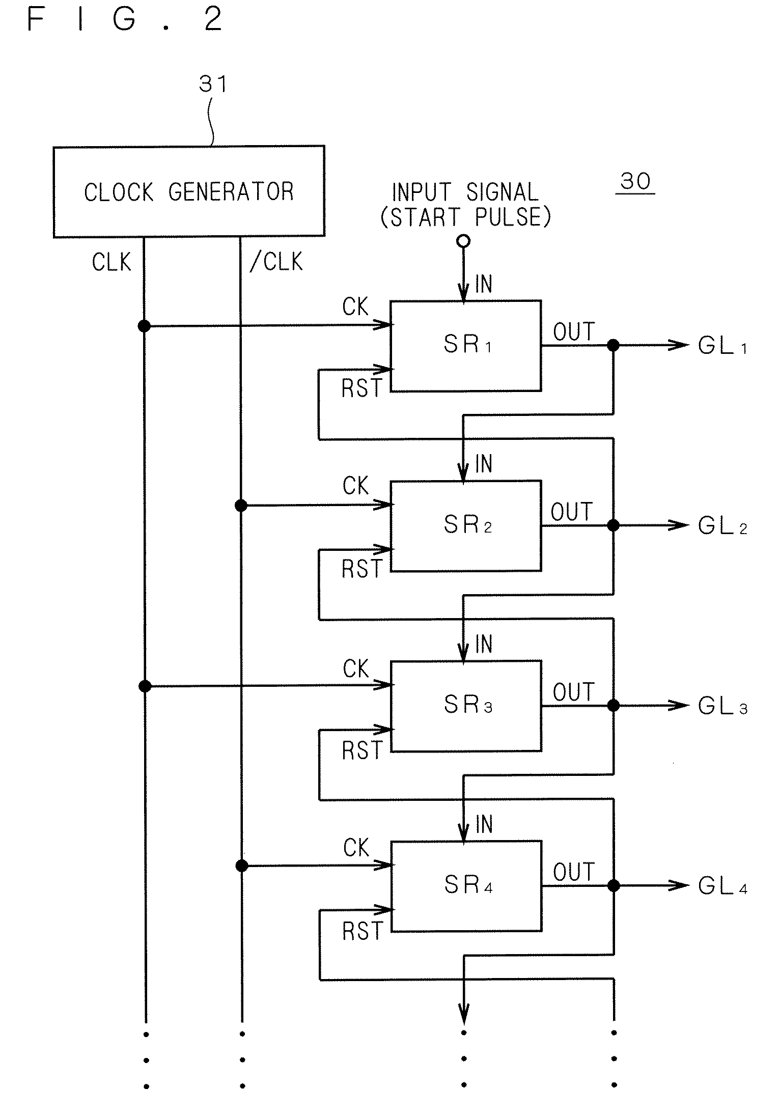
[0058]The liquid crystal display 10 comprises a liquid crystal array 20, a gate line drive circuit (scan line drive circuit) 30 and a source driver 40. Although it will be clear from the following description, a shift register according to this embodiment of the present invention is mounted on the gate line drive circuit 30.
[0059]The liquid crystal array 20 comprises a plurality of pixels 25 arranged like a matrix. Gate lines GL1, GL2, . . . (collectively called the “gate line GL”) are connected to rows of pixels (referred to as the “pixel lines” also hereinafter), respectively and data lines DL1, DL2, . . . (collectively called the “data line DL”) are connected to the columns of pixels (referred to as the “pixel columns” also hereinafter), res...
embodiment 2
[0130]According to the unit shift register SRn (FIG. 7) in the embodiment 1, the node N1 is charged by the previous stage output signal Gn−1. In other words, the output signal Gn of the unit shift register SRn is used not only for the gate line GLn, but also for charging the node N1 of the next stage unit shift register SRn+1.
[0131]The capacity component associated with the node N1 of the unit shift register SR includes the capacity of the capacity element C1 and the gate capacity of the transistor Q1. According to the embodiment 1, the capacity component becomes a part of the load capacity C3 of the output terminal OUT of the unit shift register SR, which causes the rising speed of the output signal to be lowered. This prevents the high-speed operation of the unit shift register SR.
[0132]According to an embodiment 2, a unit shift register SR that can solve the above problem is proposed. FIG. 12 is a circuit diagram of the unit shift register SR. As shown in FIG. 12, according to th...
embodiment 3
[0137]A display in which a shift register of a gate line drive circuit comprises an amorphous silicon TFT (a-Si TFT) is easy to be enlarged and has high productivity, so that it is widely used as a screen of a notebook personal computer or a big screen display.
[0138]Meanwhile, it has been known that when the gate electrode of the a-Si TFT is continuously positively biased, its threshold voltage shifts in a positive direction and its drive capability is lowered. For example, according to the circuit of the embodiment 1 (FIG. 7), since the clock signal / CLK is repeatedly inputted to the gate of the transistor Q2, there is concern that the threshold voltage of the transistor Q2 shifts and its drive capability is lowered and the output terminal OUT cannot be discharged. Thus, the electric charge that should be discharged from the node N1 through the transistor Q5 in the non-selected state is accumulated in the output terminal OUT and a defective operation in which the gate line GL to be...
PUM
 Abstract
Description
Claims
Application Information