Substrate processing apparatus, method of manufacturing a semiconductor device, and method of forming a thin film on metal surface

a technology of substrate and processing apparatus, which is applied in the direction of resistive material coating, solid state diffusion coating, natural mineral layered products, etc., can solve the problems of metal contamination in which metal is adsorption on the substrate film, and the problem of substrate contamination by fe (iron) may arise, so as to prevent the defective operation of the semiconductor device and reduce the reactivity

Active Publication Date: 2011-02-01
KOKUSA ELECTRIC CO LTD
View PDF8 Cites 2 Cited by
  • Summary
  • Abstract
  • Description
  • Claims
  • Application Information

AI Technical Summary

Benefits of technology

[0013]In the present invention, a film that has a low reactivity with reactive gases, and that can block the out diffusion of Cu, can be formed on a surface of a metallic component exposed to the inside of the processing chamber. Furthermore, this can contribute to the prevention of defective operation of the semiconductor device caused by the out diffusion of Cu.

Problems solved by technology

However, a part of a metallic component forming the furnace opening parts is exposed to the inside of the processing chamber; therefore, if out diffusion of metal from the exposed surfaces of the furnace opening parts occurs during substrate processing such as film formation or the like, metal contamination in which metal is adsorbed on the film of the substrate may occur.
For example, since the manifold of the furnace opening part is formed from stainless steel or Hastelloy, and is exposed to the inside of the reaction chamber, metals contained in the metal forming the manifold, and especially Fe, undergo out diffusion, so that the problem of contamination of the substrate by Fe (iron) may arise.

Method used


Image

  • Substrate processing apparatus, method of manufacturing a semiconductor device, and method of forming a thin film on metal surface
  • Substrate processing apparatus, method of manufacturing a semiconductor device, and method of forming a thin film on metal surface
  • Substrate processing apparatus, method of manufacturing a semiconductor device, and method of forming a thin film on metal surface

Examples


Embodiment Construction

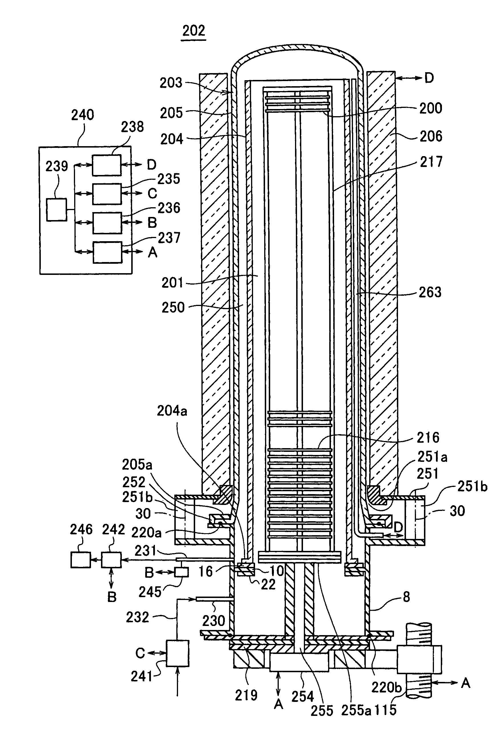
[0020]An embodiment of the present invention will be described below with reference to FIGS. 1 through 4.

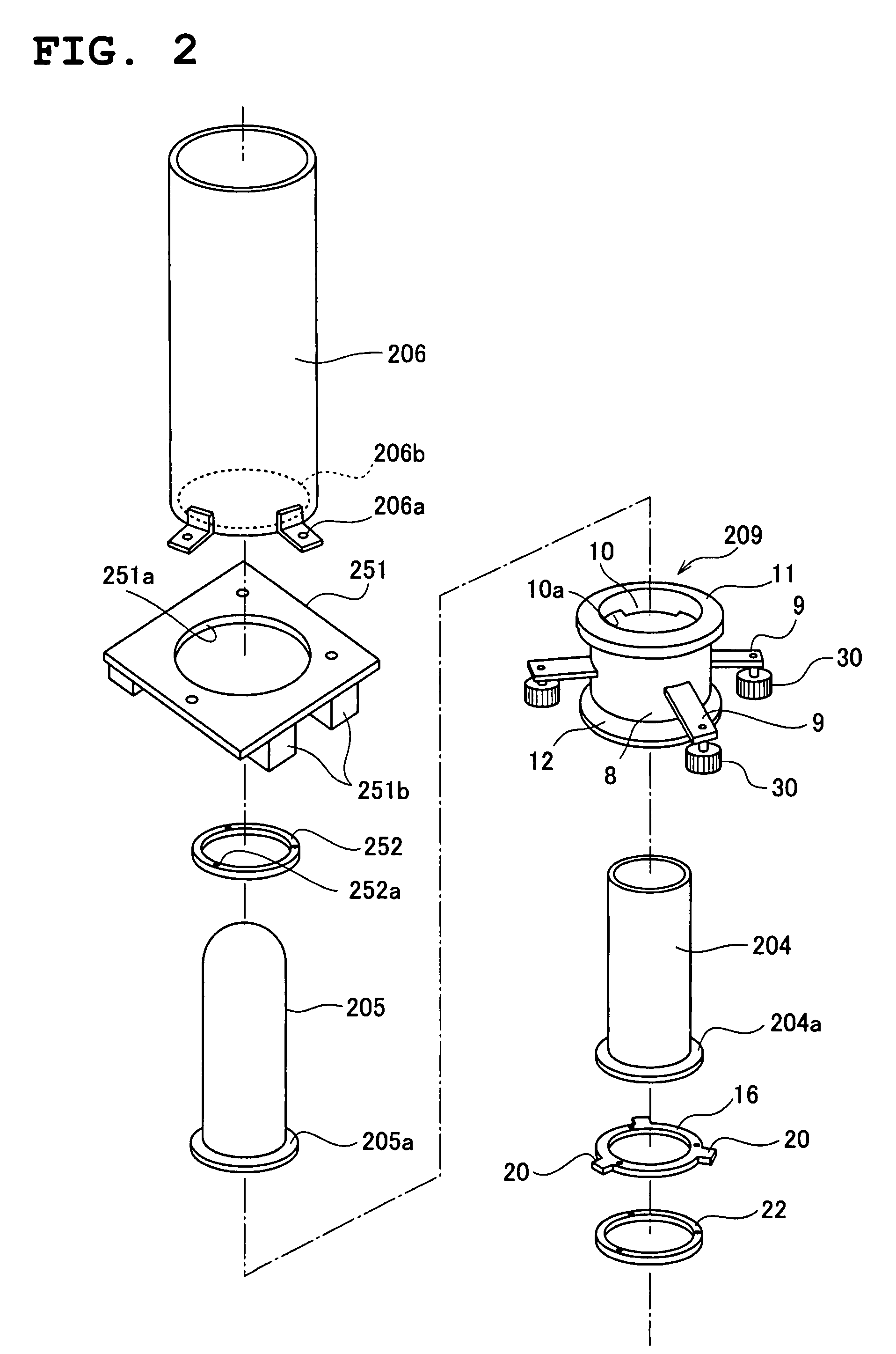
[0021]FIG. 1 is a longitudinal sectional view showing the schematic construction of the processing furnace of a substrate processing apparatus that can be appropriately used in an embodiment of the present invention. FIG. 2 is an exploded perspective view showing the construction of this substrate processing apparatus.

[0022]As is shown in FIGS. 1 and 2, a heater 206 is installed as heating means in the heating furnace 202.

[0023]The heater 206 is formed in a tubular shape that is open at the top and bottom. The heater 206 is attached in a vertical attitude via a bracket 206a to a heater base 251 used as a holding plate.

[0024]An insertion opening 251a is formed in the heater base 251 concentrically with the opening part 206b of the heater 206, and a processing tube 203 constructed from an inner tube 204 and an outer tube 205 is inserted into the heater 206 from the insertion openin...


PUM

PropertyMeasurementUnit
temperatureaaaaaaaaaa
pressureaaaaaaaaaa

Abstract

There is provided a substrate processing apparatus equipped with a metallic component, with at least a part of its metallic surface exposed to an inside of a processing chamber and subjected to baking treatment at a pressure less than atmospheric pressure. As a result of this baking treatment, a film which does not react with various types of reactive gases, and which can block the out diffusion of metals, is formed on the surface of the above-mentioned metallic component.

Description

BACKGROUND OF THE INVENTION[0001]1. Field of the Invention[0002]The present invention relates to a substrate processing apparatus and a method of manufacturing a semiconductor device using this substrate processing apparatus, and more particularly relates to a substrate processing apparatus which has a film for minimizing metal contamination, a method of manufacturing a semiconductor device, and a method of forming a thin film on a metal surface.[0003]2. Description of the Related Art[0004]Generally, in order to process a substrate in a substrate processing apparatus, the processing chamber is formed from a heat-resistant glass such as quartz, silicon carbide, or the like in order to obtain heat resistance, corrosion resistance, and reaction resistance, and the furnace opening part used to load the substrate into and out of the processing chamber is formed from stainless steel, Hastelloy, or Inconel in order to achieve heat resistance and corrosion resistance.[0005]However, a part o...

Claims


Application Information

Patent Timeline
Patent Type & Authority Patents(United States)
IPC IPC(8): C23C16/00
CPCC23C16/4404Y10T428/265Y10T428/1259H01L21/22H01L21/324
Inventor MAEDA, TAKAHIROMAEDA, KIYOHIKOOZAKI, TAKASHI
Owner KOKUSA ELECTRIC CO LTD
Why Eureka
Try Eureka