
Shift register circuit and image display comprising the same

a technology of shift register and image display, which is applied in the direction of logic circuits, digital storage, instruments, etc., can solve the problems of reducing the rising and falling speed of output signals, affecting the operation of unit shift registers, and affecting the implementation of high-speed operations. , to achieve the effect of preventing the reduction of drive capability and preventing the reduction of defective operations

Active Publication Date: 2013-07-23
TRIVALE TECH
View PDF27 Cites 46 Cited by
  • Summary
  • Abstract
  • Description
  • Claims
  • Application Information

AI Technical Summary

Benefits of technology

This present invention provides a shift register circuit that prevents defective operation when the output signal is not outputted and maintains high drive capability when the output signal is outputted. This is achieved by controlling the level of the control electrode of the first transistor so that the drive capability is not lowered while the output signal is outputted. Additionally, the switching circuit is turned on when the output signal is not outputted, which prevents the first transistor from being turned on and the output signal from becoming H level in the non- Selected period. The technical effect of this invention is that it ensures the proper operation of the shift register circuit and prevents malfunctions during the normal operation.

Problems solved by technology

Thus, when the gate potential exceeds the threshold voltage of the first transistor, the first transistor to be kept in the off state is unnecessarily turned on, which causes a defective operation of the unit shift register.
In this case, the problem is that the rising and falling speeds of the output signal are lowered and it is difficult to implement the high-speed operation.
Especially, since it is necessary to charge the gate line at high speed to activate it in order to ensure sufficient writing time of data to the pixel, in the gate line drive circuit of the display, lowering in the drive capability of the first transistor, that is, lowering in the drive capability of the unit shift register becomes a big problem.
As a result, when the drive capability of the first transistor is not sufficiently ensured, the problem the high speed operation is difficult arises again.

Method used


Image

  • Shift register circuit and image display comprising the same
  • Shift register circuit and image display comprising the same
  • Shift register circuit and image display comprising the same

Examples


embodiment 1

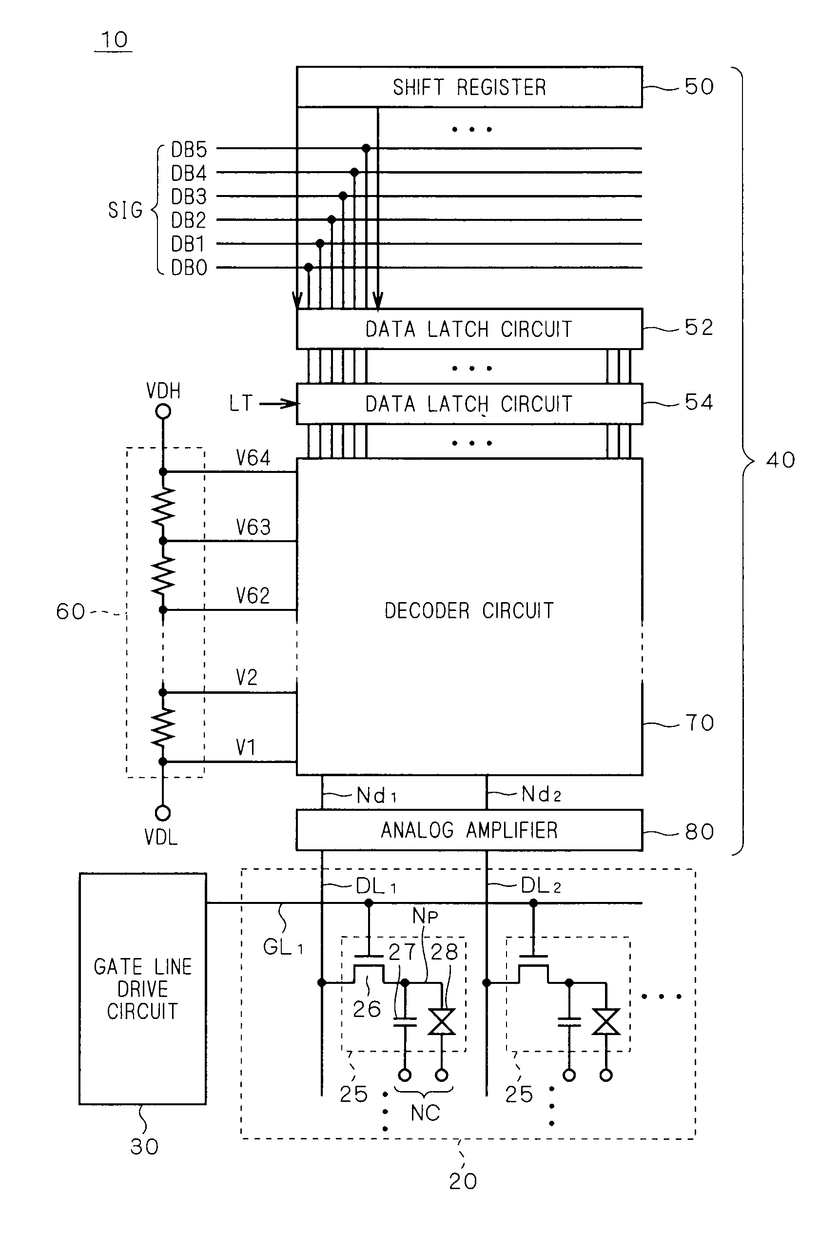
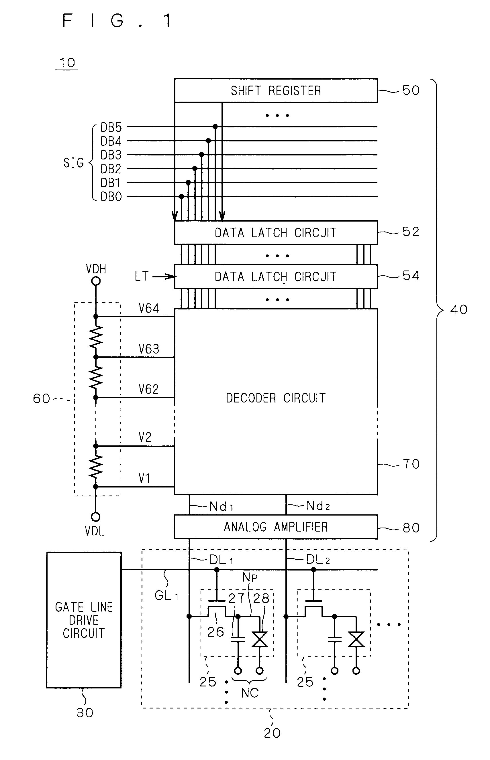
[0058]FIG. 1 is a schematic block diagram showing the constitution of a display according to the present invention and showing the whole constitution of a liquid crystal display 10 as a representative example of the display.

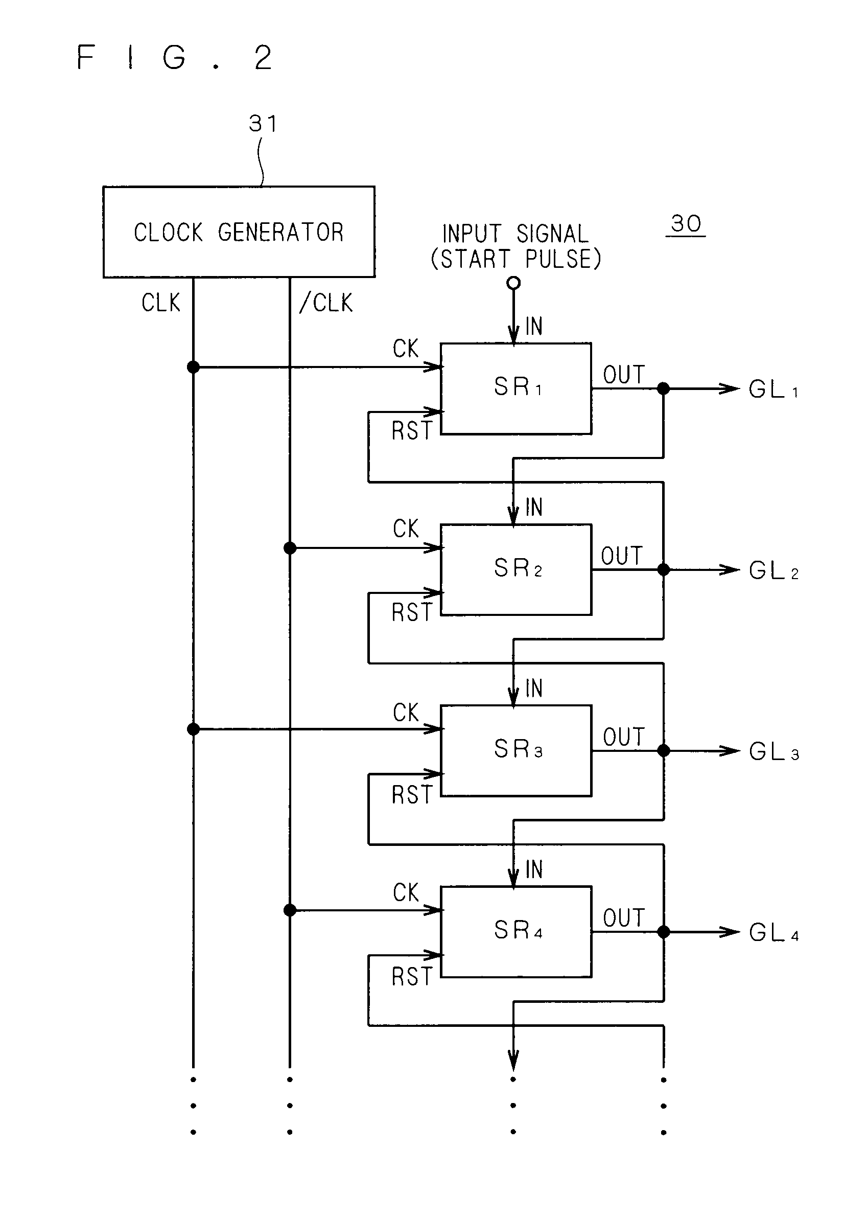
[0059]The liquid crystal display 10 comprises a liquid crystal array 20, a gate line drive circuit (scan line drive circuit) 30 and a source driver 40. Although it will be clear from the following description, a shift register according to this embodiment of the present invention is mounted on the gate line drive circuit 30.

[0060]The liquid crystal array 20 comprises a plurality of pixels 25 arranged like a matrix. Gate lines GL1, GL2, . . . (collectively called the “gate line GL”) are connected to rows of pixels (referred to as the “pixel lines” also hereinafter), respectively and data lines DL1, DL2, . . . (collectively called the “data line DL”) are connected to the columns of pixels (referred to as the “pixel columns” also hereinafter), respectively. In FIG. ...

embodiment 3

[0140]FIG. 13 is a circuit diagram showing the constitution of the unit shift register according to the As shown in FIG. 13, the source of a transistor Q2 is connected to a first clock terminal CK1. That is, the main electrode (drain) of the transistor Q2 is connected to an output terminal OUT and a clock signal CLK having a phase different from that of a clock signal / CKL to be inputted to a control electrode (gate) is supplied to another main electrode (source).

[0141]According to this constitution, when the clock signal / CLK inputted to the gate of the transistor Q2 becomes L level and the transistor Q2 is turned off, since the clock signal CLK inputted to the source becomes H level, a state equivalent to a case where the gate of the transistor Q2 is negatively biased with respect to the source is provided. Thus, since a threshold voltage that shifted in the positive direction returns in the negative direction and makes a recovery, there is an effect that the drive capability of ...

embodiment 5

[0169]FIG. 17 is a circuit diagram showing the unit shift register according to the According to the unit shift register SR shown in FIG. 17, the gate of a transistor Q5 and a first clock terminal CK1 are not directly connected and a level adjustment circuit 100 is interposed therebetween. The level adjustment circuit 100 lowers the H level of a clock signal inputted to the first clock terminal CK1 by a predetermined value (reduces the absolute value of the H level based on L level) and then supplies it to the gate of the transistor Q5. That is, the level adjustment circuit 100 functions to reduce the amplitude of the clock signal inputted to the first clock terminal CK1 by the predetermined value.

[0170]The level adjustment circuit 100 in the example shown in FIG. 17 comprises transistors Q9 and Q10. When it is assumed that the node connected to the gate of the transistor Q5 is defined as node N3, the transistor Q9 (third transistor) is connected between the node N3 and the first c...


PUM


Abstract

In a shift register circuit, a defective operation while an output signal is not outputted and a drive capability lowering while the output signal is outputted are prevented. A unit shift register comprises a first transistor for supplying a clock signal inputted to a first clock terminal to an output terminal, and the first transistor is driven by a drive circuit. A second transistor is connected between the gate of the first transistor and the output terminal and has a gate connected to the first clock terminal. The second transistor connects the gate of the first transistor to the output terminal based on the clock signal when the gate of the first transistor is at L (Low) level.

Description

CROSS-REFERENCE TO RELATED APPLICATIONS[0001]This application is a divisional of U.S. application Ser. No. 11 / 739,399, filed Apr. 24, 2007, the contents of which are incorporated herein by reference, and is based upon and claims the benefit of priority from prior Japanese Patent Application Nos. 2006-120118, filed Apr. 25, 2006 and 2007-028894, filed Feb. 8, 2007.BACKGROUND OF THE INVENTION[0002]1. Field of the Invention[0003]The present invention relates to a shift register circuit and more particularly, to a shift register circuit used in such as a scan line drive circuit in an image display and comprising only the same conductivity type field effect transistor.[0004]2. Description of the Background Art[0005]According to an image display such a liquid crystal display (referred to as the “display” hereinafter), a gate line (scan line) is provided with respect to each pixel row (pixel line) of a display panel in which a plurality of pixels are arranged like a matrix, and the display...

Claims


Application Information

Patent Timeline
Patent Type & Authority Patents(United States)
IPC IPC(8): G09G3/36
CPCG09G3/3677G11C19/28G09G2300/0408G09G2310/027G09G2310/08G09G2310/0267G09G3/20G09G3/36G11C19/00H03K19/00
Inventor TOBITA, YOUICHI
Owner TRIVALE TECH
Learn More