Semiconductor device, manufacturing method of semconductor device, manufacturing equipment of semiconductor device, light emitting diode head, and image forming apparatus

a technology of semiconductor devices and manufacturing methods, applied in the direction of semiconductor devices, electrical devices, basic electric elements, etc., can solve the problems of adversely limiting the number of semiconductor devices made from a single semiconductor wafer, and achieve the effect of reducing the occurrence of chipping, reducing the margin area, and increasing the area ratio

Inactive Publication Date: 2007-10-25
OKI DATA CORP
View PDF9 Cites 51 Cited by
  • Summary
  • Abstract
  • Description
  • Claims
  • Application Information

AI Technical Summary

Benefits of technology

[0007]To solve such problems, the present invention provides a semiconductor device comprising a semiconductor element area arranged on a first substrate, wherein an etching process etches at least a portion of the first substrate to separate the semiconductor device from another neighboring semiconductor device. The present invention surely reduces occurrence of chipping by employing the required etching process as a separation method between devices instead of the conventional dicing process.
[0010]The present invention further provides a manufacturing method of a semiconductor device in which a first substrate comprising a semiconductor element area is divided into a plurality of semiconductor devices, the manufacturing method comprising steps of performing a first etching process to etch a separation area on a front surface of the first substrate, coating with a thin film a non-etching area including a sidewall of the etched separation area and excluding an aperture area on a bottom of the etched separation area on the front surface of the first substrate, performing a second etching process to etch the front surface of the first substrate through the aperture area as an etching window, arranging a supporter on the front surface of the first substrate to prevent the plurality of semiconductor devices from coming apart after the first substrate is divided, and grinding a back surface of the first substrate to cause a hollow portion etched by the first and second etching process to penetrate through the front surface to the back surface of the first substrate.
[0012]The semiconductor device according to the present invention surely reduces occurrence of chipping by employing the etching process as a separation method between devices instead of the conventional dicing method. Therefore, the present invention is capable of making smaller a margin area for chipping around the semiconductor device, and making higher a ratio of an area in which the semiconductor devices can be formed to an area for manufacturing step, and thereby, the present invention increases the number of devices that can be manufactured.

Problems solved by technology

In the dicing method, the wafer is cut by the dicing blade which adversely impacts the wafer, and such an impact is likely to chip end portions of the semiconductor device, namely, to cause chipping.
There exists a problem that the above-mentioned dicing method requires a relatively large area between semiconductor devices to adversely limit the number of semiconductor devices made from a single semiconductor wafer.

Method used


Image

  • Semiconductor device, manufacturing method of semconductor device, manufacturing equipment of semiconductor device, light emitting diode head, and image forming apparatus
  • Semiconductor device, manufacturing method of semconductor device, manufacturing equipment of semiconductor device, light emitting diode head, and image forming apparatus
  • Semiconductor device, manufacturing method of semconductor device, manufacturing equipment of semiconductor device, light emitting diode head, and image forming apparatus

Examples


first embodiment

[0036]The first embodiment discloses a manufacturing method of a semiconductor device with the use of a silicon wafer. The first embodiment is especially advantageous for forming many semiconductor light emitting elements, such as, e.g., LED array chips, at a time.

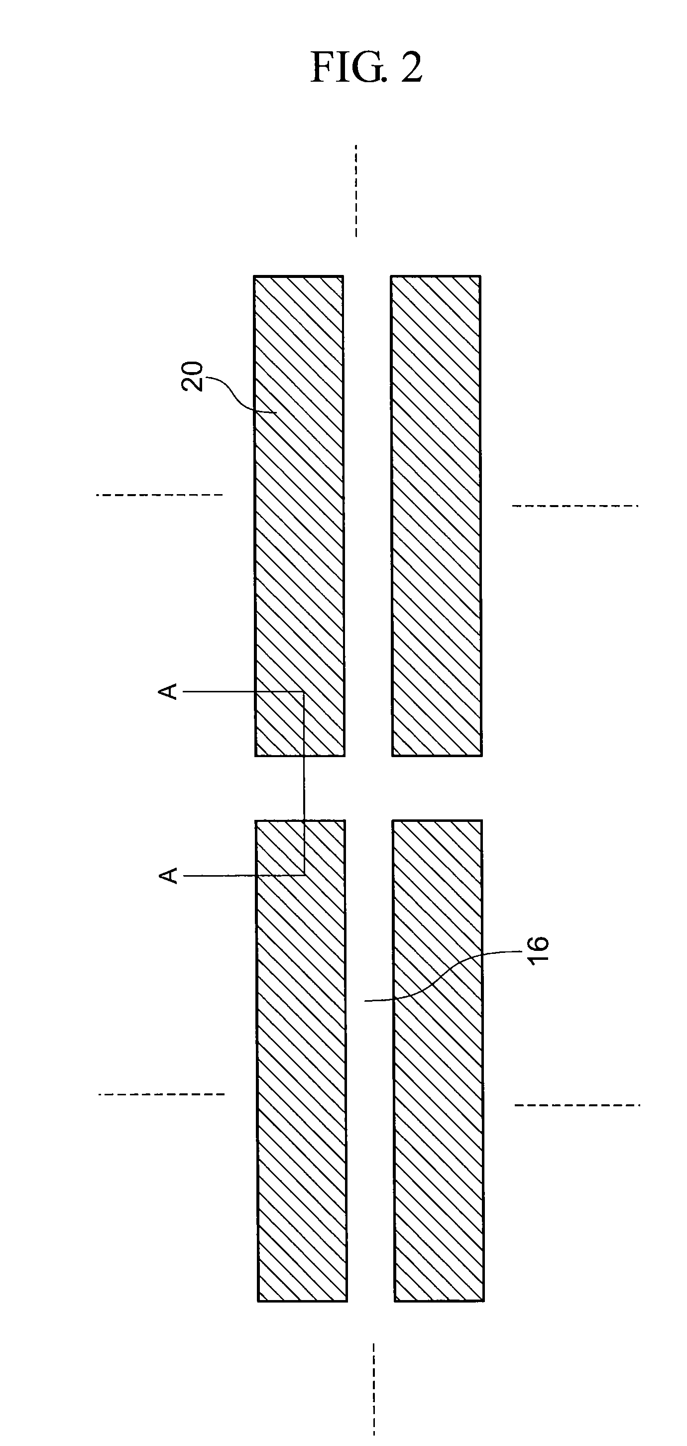
[0037]In the first embodiment, semiconductor element areas 20 each in a rectangular shape are formed to line up in a lateral and longitudinal direction as shown in FIG. 2. Each of the semiconductor element areas 20 in a rectangular shape are formed on a silicon substrate 11, namely, a semiconductor wafer. An area between the semiconductor element areas 20 in a rectangular shape is a separation area 16 that is to be etched for separating the semiconductor element areas 20 into individual devices. Particularly in the first embodiment, the separation area 16 is a belt-like area extending in a grid.

[0038]After a required semiconductor device has been formed, namely, for example, an electrode layer, an active layer, and the lik...

second embodiment

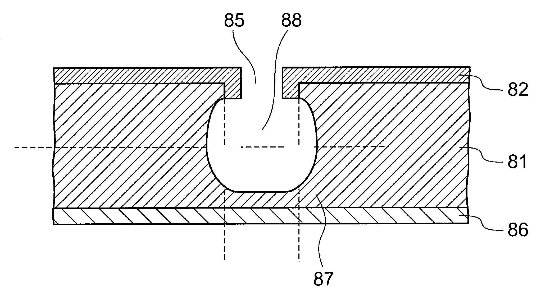
[0046]FIG. 5 is a diagram showing a cross section of the wafer after the separation area has been etched through the manufacturing method according to the second embodiment and before each of the devices is separated. The masking material layer 32 is formed on the surface of a silicon substrate 31. Then, with the help of the masking material layer 32, an aperture area 35 of a narrow width is formed from a surface 44 to a depth 43 in a same manner as the first embodiment. On a sidewall of the aperture area 35, a sidewall protection layer 32a is formed to incorporate with the surface 32b.

[0047]Below the narrow aperture area 35, a hollow space 36 (separation area) in a dome shape is formed through the isotropic etching process. A larger amount of the wafer is removed in a hollow space 36 than in the aperture area 35, and thus a sidewall 36w in the hollow space 36 is in a shape further etching the wafer than the width of the aperture area 35.

[0048]In order to obtain the above-mentioned...

third embodiment

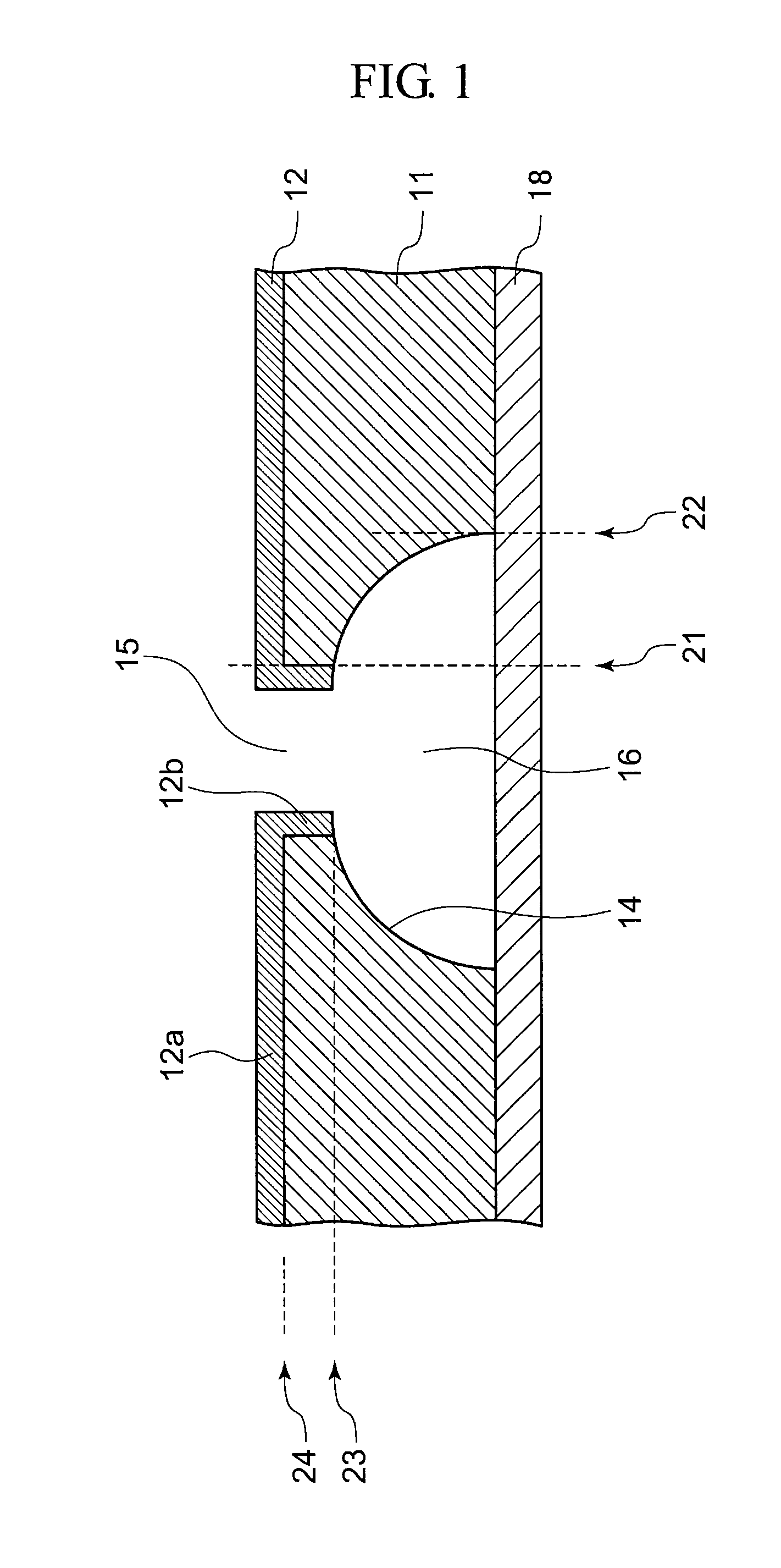
[0053]FIG. 9 and FIG. 10 are cross sections of the wafer showing steps of the manufacturing method of the semiconductor device according to the third embodiment of this invention. First, as shown in FIG. 9, a masking material layer 52 is formed on a silicon substrate 51 except a separation area 56 that is to be left uncovered. Then, the anisotropic etching process forms an aperture area 55 at a location corresponding to the location of the separation area 56 from a surface 54 to a depth 53. The anisotropic etching process forms a substantially vertical sidewall on an edge position 57 of the aperture area 55.

[0054]Subsequently, as shown in FIG. 10, a second masking material layer 60 is formed on the back surface of the substrate except the separation area 56, namely, an area that is to be etched to form an etching aperture area 60a on the back surface of the wafer. After forming the etching aperture area 60a as mentioned above on the second masking material layer 60, a chip fixation ...


PUM


Abstract

A manufacturing method of a semiconductor device is provided to manufacture an increased number of semiconductor devices per single substrate such as, e.g., a wafer while obviating damages like those caused by conventional dicing method.The manufacturing method comprises steps of performing a first etching process to etch a separation area on a front surface of a substrate, arranging a supporter on a back surface of the first substrate to prevent semiconductor devices from coming apart, coating with a thin film a non-etching area including a sidewall of the etched separation area and excluding a bottom of the etched separation area on the front surface of the first substrate, and performing a second etching process to etch the first substrate from the front surface through an area not coated by the thin film to divide the substrate into multiple semiconductor devices.

Description

BACKGROUND OF THE INVENTION[0001]1. Field of the Invention[0002]This invention generally relates to devices and methods such as a semiconductor device formed by dividing a semiconductor element area formed on a substrate and a manufacturing method of the semiconductor device. This invention more particularly relates to a semiconductor device separated from another semiconductor device under the use of etching technology, a manufacturing method of the semiconductor device, a manufacturing equipment of the semiconductor device, a light emitting diode head, and an image forming apparatus.[0003]2. Description of Related Art[0004]There has been conventionally known a dicing method for separating multiple semiconductor devices formed on a semiconductor wafer into individual semiconductor devices (chips). In the dicing method, the wafer is cut by the dicing blade which adversely impacts the wafer, and such an impact is likely to chip end portions of the semiconductor device, namely, to cau...

Claims


Application Information

Patent Timeline
IPC IPC(8): H01L21/302
CPCH01L21/3065H01L21/6836H01L2221/68327H01L33/0095H01L21/78
Inventor OGIHARA, MITSUHIKO
Owner OKI DATA CORP
Why Eureka
Try Eureka