Semiconductor Device and Method for Manufacturing the Same

Inactive Publication Date: 2007-11-08
NEC CORP
View PDF6 Cites 139 Cited by
  • Summary
  • Abstract
  • Description
  • Claims
  • Application Information

AI Technical Summary

Benefits of technology

[0070] The present invention can provide a semiconductor device having a dense SR

Problems solved by technology

However, the SRAM cell disadvantageously requires a larger cell area because of the need for six transistors for one memory cell, t

Method used


Image

  • Semiconductor Device and Method for Manufacturing the Same
  • Semiconductor Device and Method for Manufacturing the Same
  • Semiconductor Device and Method for Manufacturing the Same

Examples


Embodiment Construction

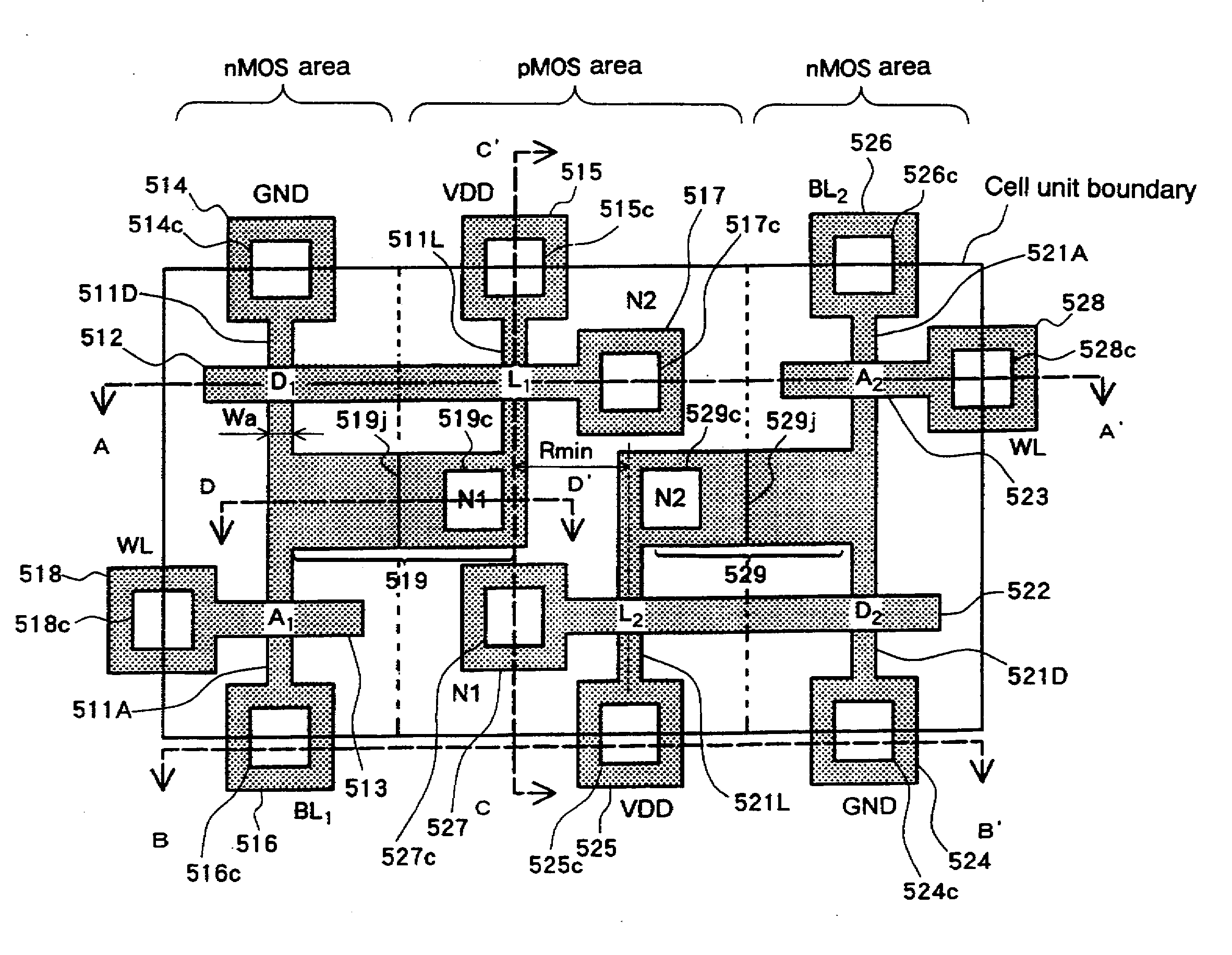
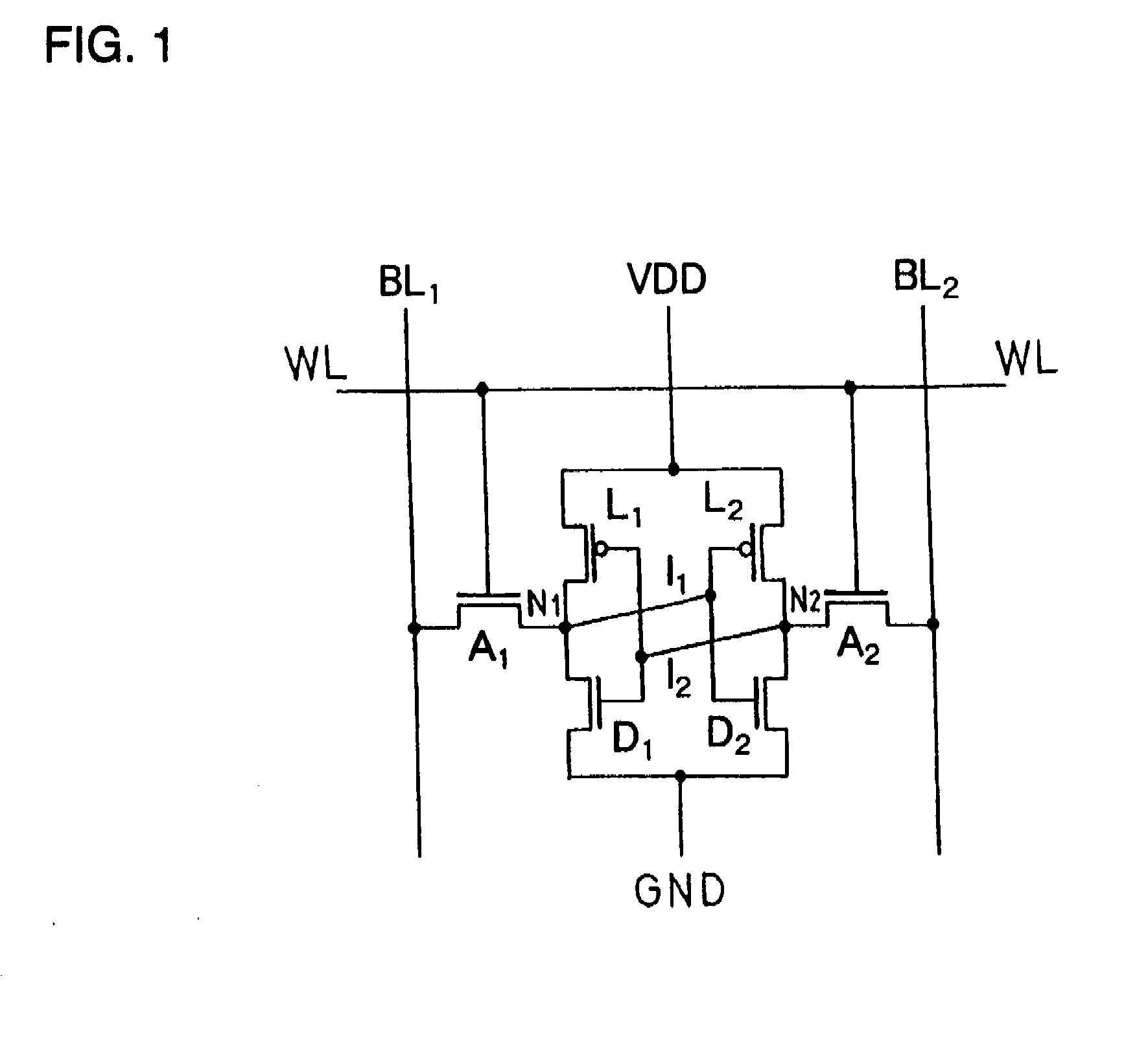
[Configuration of a FIN Type FET]

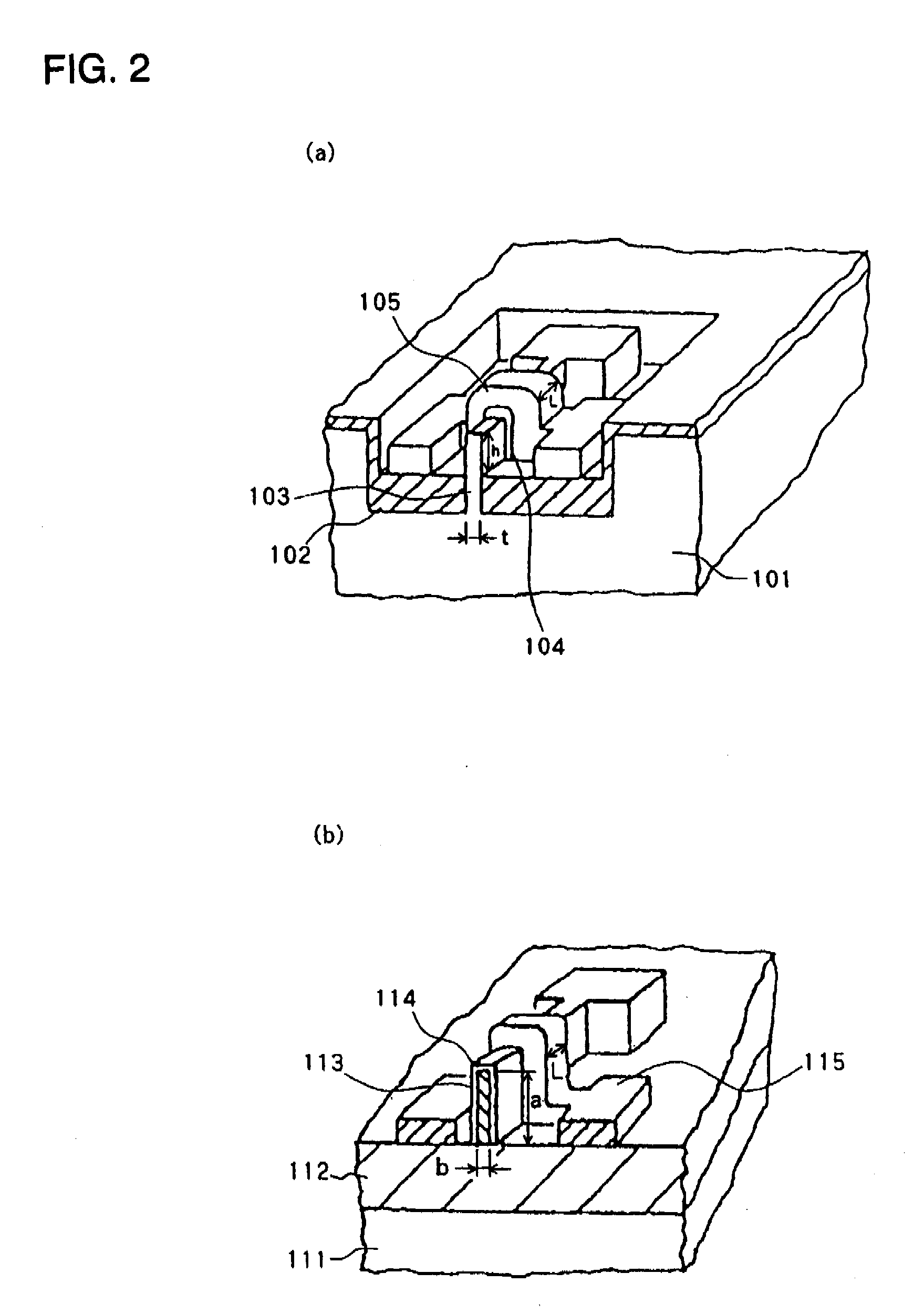
[0090] A FIN type FET that is applied to a SRAM structure according to the present invention may be a field effect transistor having a semiconductor layer 303 that projects upward perpendicularly to a substrate plane, a gate electrode 304 that extends on the opposite sides of the semiconductor layer so as to stride over its top, a gate insulating film 305 interposed between the gate electrode 304 and the semiconductor layer 303, and a source / drain area 306 formed in the semiconductor layer 303, for example, as shown in FIG. 4.

[0091] The semiconductor layer (hereinafter referred to as a “projecting semiconductor layer”) projecting upward perpendicularly to the substrate plane, constituting the FIN type FET, may be provided on a base insulating film 302 on a semiconductor substrate 301, for example, as shown in FIG. 4. In the present invention, the substrate plane is an arbitrary surface parallel to the substrate, in this case, the surface of the bas...


PUM


Abstract

A semiconductor device having SRAM cell units each comprising a pair of driving transistors, a pair of load transistors and a pair of access transistors, in which each of the transistors has a semiconductor layer projecting upward from a substrate plane, a gate electrode extending on opposite sides of the semiconductor layer so as to stride over a top of the semiconductor layer, a gate insulting film interposed between the gate electrode and the semiconductor layer, and a pair of source/drain areas formed in the semiconductor layer; a longitudinal direction of each semiconductor layer extends along a first direction; and between the adjacent SRAM cell units in the first direction, the semiconductor layer in one of the corresponding transistors is located on a center line of the semiconductor layer in the other transistor which center line extends along the first direction.

Description

TECHNNICAL FIELD [0001] The present invention relates to a semiconductor device and a method for manufacturing this semiconductor device, and in particular, to a semiconductor storage device comprising a SRAM (Static Random Access Memory) and a method for manufacturing this semiconductor device. BACKGROUND ART [0002] SRAM memory cells that are semiconductor storage elements have a basic structure described below. [0003] As shown in a circuit diagram in FIG. 1, the SRAM memory cell is composed of a flip flop circuit serving as an information storage section, and a pair of access transistors A1 and A2 which controls the conduction between and the flip flop circuit and data lines (bit lines BL1 and BL2) through which information is written or read. The flip flop circuit is composed of, for example, a pair of CMOS inverters each composed of one driving transistor D1 (D2) and one load transistor L1 (L2). [0004] One of source and drain areas of the access transistor A1 (A2) is connected t...

Claims


Application Information

Patent Timeline
IPC IPC(8): H01L21/8244H01L21/82H01L21/84H01L21/86H01L27/11H01L27/12H01L29/786
CPCH01L21/84H01L21/86H01L27/11H01L29/785H01L27/1108H01L27/1203H01L27/1104H10B10/125H10B10/00H10B10/12
Inventor TAKEDA, KOICHIWAKABAYASHI, HITOSHITAKEUCHI, KIYOSHIYAMAGAMI, SHIGEHARUNOMURA, MASAHIROTANAKA, MASAYASUTERASHIMA, KOICHIKOH, RISHOTANAKA, KATSUHIKO
Owner NEC CORP
Why Eureka
Try Eureka