Methods of forming blind wafer interconnects, and related structures and assemblies

a technology of blind wafers and interconnects, applied in the direction of semiconductor devices, semiconductor/solid-state device details, electrical apparatus, etc., can solve the problems of increasing the propensity for wire damage, and affecting the production of miniature semiconductor devices. , to achieve the effect of reducing processing time and expens

Inactive Publication Date: 2007-11-08
ROUND ROCK RES LLC
View PDF7 Cites 68 Cited by
  • Summary
  • Abstract
  • Description
  • Claims
  • Application Information

AI Technical Summary

Benefits of technology

[0016] The present invention, in a number of embodiments, comprises methods for making small-diameter blind-wafer interconnects (BWIs) in substrates such as semiconductor wafers. More specifically, the methods pertain to the formation of a blind hole, and formation of a passivating layer on the back surface of a substrate and interior hole surfaces prior to filling the blind hole with solder or other conductive material. The blind hole may be formed by etching, laser ablation, mechanical drilling, or a combination of such techniques. In one embodiment, CMP may be utilized to remove excess photoresist and metal seed material from the substrate back side, without entrapping particles in the blind hole. The blind wafer interconnects (BWIs) formed by methods of the invention may be used to electrically connect conductors on the back side of a substrate to conductors, e.g., bond pads, on the front side (i.e., active surface) thereof. The entire BWI-forming process may be completed at the wafer level, to reduce both processing time and expense. The invention alleviates the afore-stated problems in forming blind wafer interconnects by conventional methods.
[0018] The methods of the present invention may be generally described, infra, in the context of forming a blind wafer interconnect (BWI) in a substrate such as a semiconductor wafer in an intermediate stage of manufacture, i.e., following circuit fabrication but before die singulation and packaging. Thus, BWIs may be formed following the creation of multiple identical integrated circuits (ICs), including bond pads or other conductive terminals on the first or active surface of a semiconductor wafer. The methods of the present invention are particularly suited to forming BWIs in a wafer which has already been thinned to a final thickness. More particularly, these methods may be particularly useful for connecting an existing bond pad or other conductor on a first (active) surface with conductors to be formed on a second (back side) surface of the substrate or to another substrate closely spaced from the back side surface. The method obviates the use of wire bonds and enables the formation of high density devices. The present invention also includes electronic apparatus, optoelectronic devices and the like incorporating blind wafer interconnects formed by methods of the invention.
[0023] The methods of the invention offer substantial advantages over the prior art. Each of the acts in the method of the present invention uses known and well-developed technology. The method enables the production of high density BWI arrays without the aforementioned problems known in the prior art. Furthermore, BWI formation according to the present invention may be conducted at the wafer stage, whereby each act of the method may be simultaneously applied to all of the individual semiconductor devices on the wafer.

Problems solved by technology

One of the critical limitations in the production of miniature semiconductor devices relates to electrical conductors for connection of their integrated circuit(s) to an apparatus such as a circuit board or another die.
Connection of these bond pads to another device or circuit board may conventionally utilize fine wires, commonly termed wire bonds, which are subject to displacement (leading to short-circuits with other conductors) and breakage (leading to open circuits).
Despite having a relatively long history of widespread use in the industry, wire-bonding remains a time-consuming and expensive process.
The propensity to wire damage is increased as the devices become more miniaturized and dense.
Where a plurality of individual dice are joined to form a multi-chip module (MCM), wiring costs and high rates of wire damage represent particularly substantial problems.
Further, wire bonds exhibit undesirably high inductance, 5 nh being typical.
The CMP results in a bare semiconductor (e.g., silicon) surface which closely abuts the conductive via, leading to potential short-circuiting to the substrate material when a solder ball or other conductor is joined to the conductive via end.
Overall, this method requires numerous acts, is costly, and may not achieve the desired reliability.
This method may sometimes result in other problems, including molten / softened solder drainage from the via due to gravity and replacement by solder from the adjacent solder ball.
While a circuit board is typically manufactured at a desired final thickness, semiconductive materials such as silicon and the like are fragile materials, subject to easy fracture.

Method used


Image

  • Methods of forming blind wafer interconnects, and related structures and assemblies
  • Methods of forming blind wafer interconnects, and related structures and assemblies
  • Methods of forming blind wafer interconnects, and related structures and assemblies

Examples


Embodiment Construction

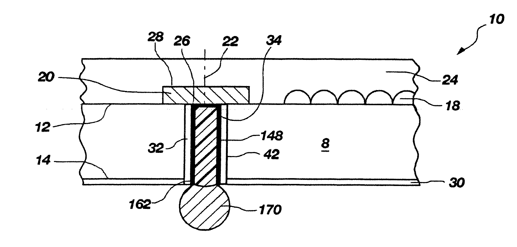
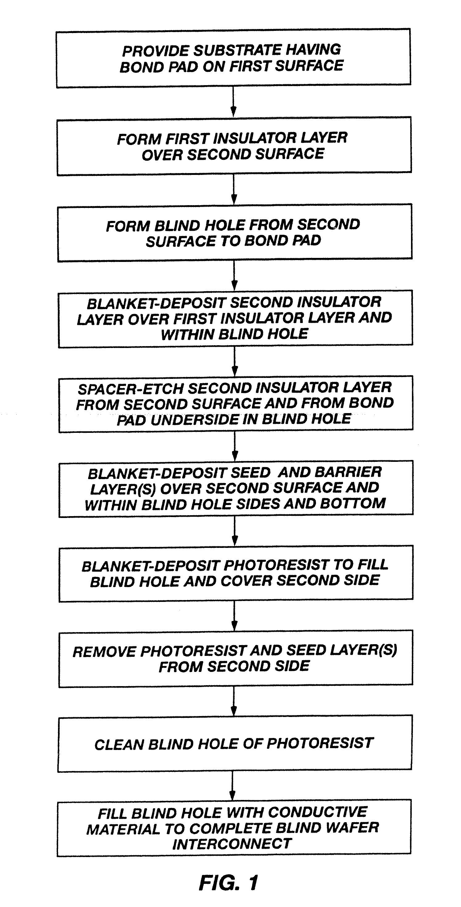
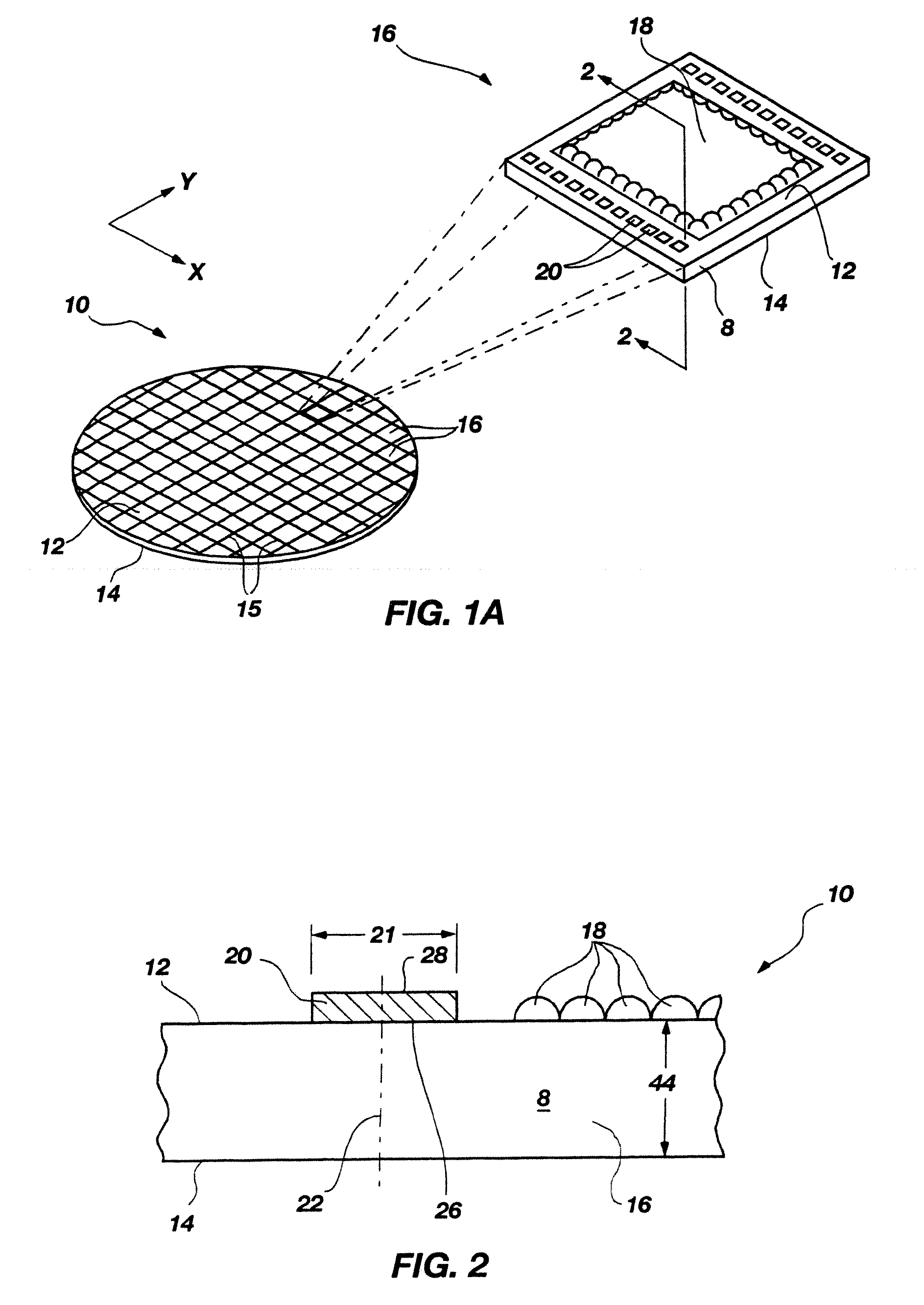
[0056] The invention comprises methods for forming blind vias (“BVs”) also known as blind wafer interconnects (“BWIs”), which penetrate into a second surface of a semiconductor substrate structure, typically to contact bond pads or other conductors on the first surface. Referring to FIG. 1A, the first surface may be an active surface 12 of a wafer 10 or other bulk semiconductor substrate and the second surface is a wafer back side surface 14. The term “via” is a general term denoting a conductor passing into or through a semiconductor substrate structure substantially transverse to a major plane of the substrate. The term “blind wafer interconnect” is often used more specifically where the substrate structure is a wafer (see FIG. 1A) or other bulk substrate of semiconductor material. In this application, the terms will be used interchangeably as applying to any substrate material comprising a layer of semiconductor material and which may be subjected to a thinning process for reduci...


PUM


Abstract

Methods for forming blind wafer interconnects (BWIs) from the back side surface of a substrate structure to the underside of a bond pad on the opposing surface includes the formation of a blind hole from the back side surface, forming a passivating layer therein, removing passivation material from the blind hole bottom, depositing at least one conductive layer within the blind hole, and filling the blind hole with solder or other conductive material or a dielectric material.

Description

CROSS-REFERENCE TO RELATED APPLICATION [0001] This application is a continuation of application Ser. No. 11 / 219,315, filed Sep. 1, 2005, pending. The disclosure of the previously referenced U.S. patent application is hereby incorporated by reference in its entirety.BACKGROUND OF THE INVENTION [0002] 1. Field of the Invention [0003] The present invention relates to semiconductor devices and fabrication methods therefor. More particularly, the invention pertains to methods for forming conductive blind vias (blind wafer interconnects) in a substrate such as a semiconductor wafer or other substrate, and related structures and assemblies. [0004] 2. Background of Related Art [0005] Semiconductor devices that have integrated circuits are produced by fabricating a large plurality of identical circuit patterns on a semiconductor wafer or other bulk semiconductor substrate. Each circuit pattern defines the location of a semiconductor die, there being circuit-devoid areas, commonly termed “str...

Claims


Application Information

Patent Timeline
Patent Type & Authority Applications(United States)
IPC IPC(8): H01L21/44
CPCH01L21/76898H01L25/0657H01L2924/0002H01L2924/00014H01L2224/0401H01L2224/16H01L2224/05572H01L25/50H01L2225/06513H01L2225/06541H01L2924/15311H01L2224/16225H01L2224/05009H01L2224/0557H01L2224/06181H01L2224/13022H01L2224/13025H01L2224/16146H01L2224/16227H01L2924/00012H01L2224/05552
Inventor AKRAM, SALMANRIGG, SIDNEY B.
Owner ROUND ROCK RES LLC
Why Eureka
Try Eureka