Semiconductor chip for driving light emitting element, light emitting device, and lighting device

a technology semiconductor chips, which is applied in the direction of static indicating devices, instruments, electroluminescent light sources, etc., can solve the problems of light emitting elements that are likely to be broken, and achieve the effects of high reliability, small mounting area, and high resistance to pressur

Inactive Publication Date: 2007-11-08
PANASONIC CORP
View PDF2 Cites 30 Cited by
  • Summary
  • Abstract
  • Description
  • Claims
  • Application Information

AI Technical Summary

Benefits of technology

[0064] The invention has an outstanding effect of realizing a light emitting device having a small mounting area.
[0065] The invention realizes an inexpensive light emitting device having high reliability by eliminating a protective element such as a zener diode required in the prior art.
[0066] The invention realizes a light emitting device that makes high capacity to resist pressure of electrostatic breakdown of external connection terminals of a luminous module.
[0067] In the light emitting device of the invention, since light emitting elements are mounted on the driver IC chip, as compared with the prior art, parasitic resistance and stray capacitance of substrate wiring are reduced. As a result, it is easy to design the phase compensation for stabilizing a current value. The invention has an effect that luminance of light is stable and flickering of light is eliminated.
[0068] The invention realizes an inexpensive semiconductor chip for driving light emitting elements that can be combined with an arbitrary number of light emitting elements.
[0069] The invention realizes an inexpensive lighting device.

Problems solved by technology

Since visible light emitting diodes and other light emitting elements are likely to be broken by static electricity or voltage, protective elements are needed.

Method used


Image

  • Semiconductor chip for driving light emitting element, light emitting device, and lighting device
  • Semiconductor chip for driving light emitting element, light emitting device, and lighting device
  • Semiconductor chip for driving light emitting element, light emitting device, and lighting device

Examples


embodiment 1

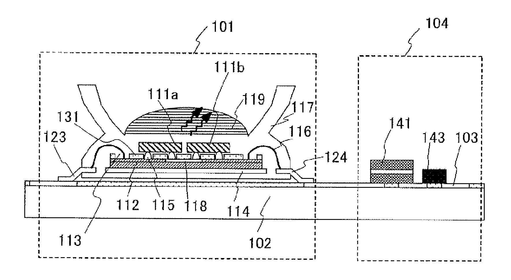
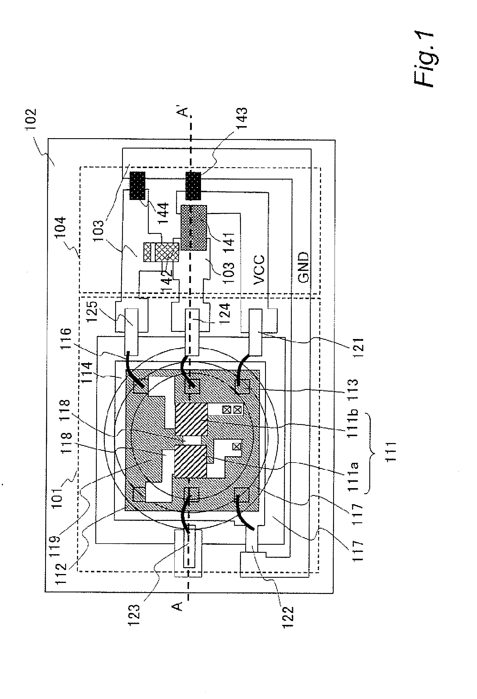
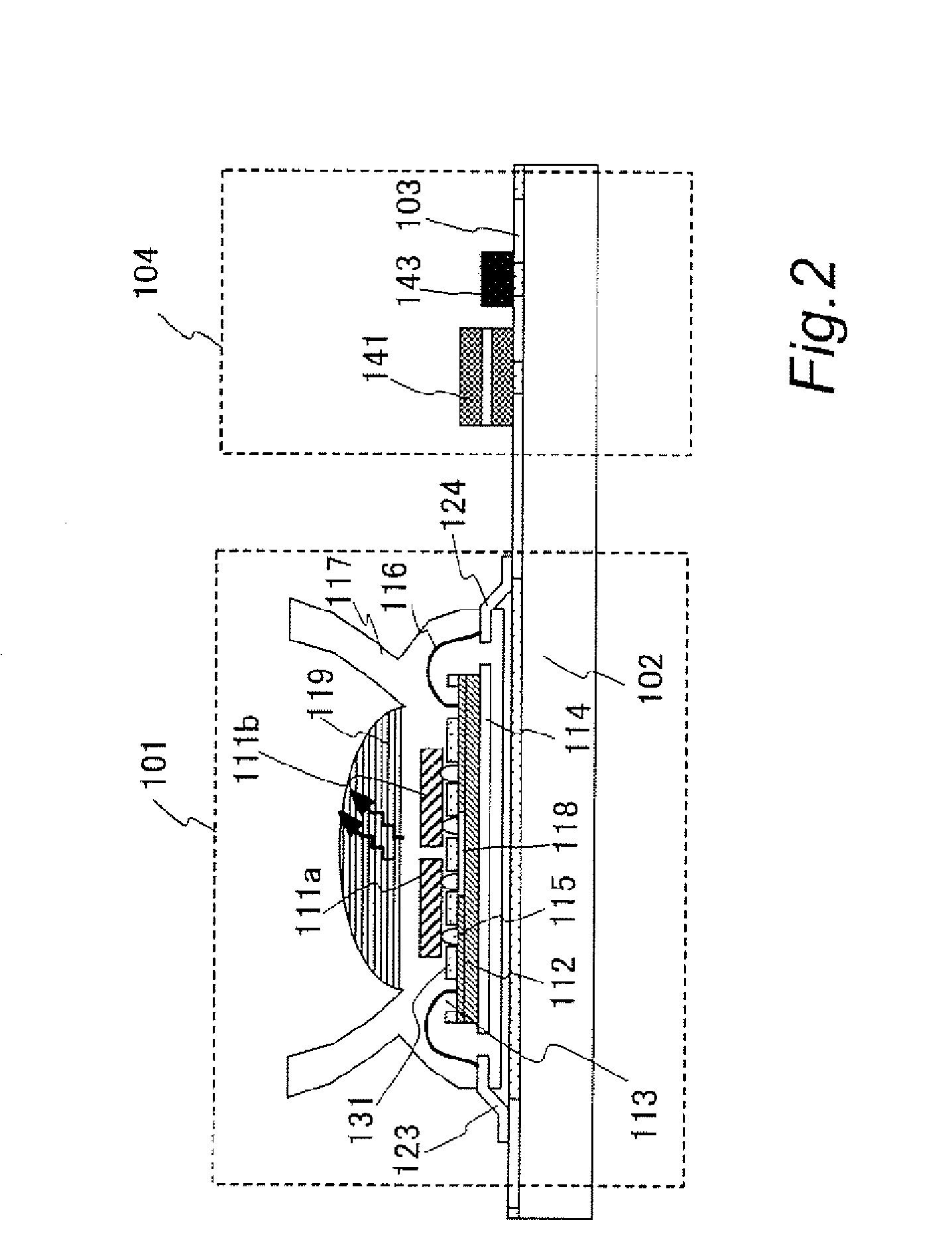
[0087] Referring to FIG. 1 to FIG. 5, a light emitting device in an embodiment 1 of the invention is described below. FIG. 1 is a plan view of structure of the light emitting device in the embodiment 1 of the invention. FIG. 2 is a sectional view along broken line A-A′ in FIG. 1. FIG. 3 is a partial magnified sectional view of a driver IC chip 112. FIG. 4 is a plan view showing shapes of aluminum wirings for connecting light emitting elements 111a and 111b being LED and the driver IC chip 112. FIG. 5 is a circuit diagram of the light emitting device in the embodiment 1 of the invention. In FIG. 1 to FIG. 5, same elements are identified with same reference numerals. In FIG. 1 to FIG. 5, same elements as FIG. 12 to FIG. 14 in the prior art are identified with same reference numerals.

[0088] In FIG. 1 and FIG. 2, the light emitting device in embodiment 1 of the invention is described. The light emitting device in embodiment 1 of the invention has substrate wirings 103 (including a VCC ...

embodiment 2

[0134] Referring to FIG. 6, a light emitting device in an embodiment 2 is explained. FIG. 6 is a circuit diagram of the light emitting device in the embodiment 2. In FIG. 6, same elements as in FIG. 5 are identified with same reference numerals. What the light emitting device in the embodiment 2 differs from the light emitting device in the embodiment 1 lies in that four light emitting elements 111 (111a, 111b, 111c, and 111d) are connected in series. Other structure is same as in the embodiment 1. Hence, duplicate explanation is omitted. In embodiment 2, since essential parts are identical, same effects as in the embodiment 1 are obtained.

[0135] The number and connection of light emitting elements 111 are not limited to the embodiment 1 or the embodiment 2, but an arbitrary number of light emitting elements may be connected, or plural light emitting elements and series resistors can be connected in parallel. The invention may be also realized by using only one light emitting eleme...

embodiment 3

[0137] Referring to FIG. 7, a light emitting device in the embodiment 3 is explained. The light emitting device in the embodiment 3 differs from embodiment 1 (FIG. 5) only in the structure of the first protective circuit 501. FIG. 7 is a circuit diagram of the protective circuit of the light emitting device in the embodiment 3. The first protective circuit 501 in the embodiment 3 has a zener diode 711 and a diode 712 which are connected in parallel.

[0138] The diode 712 is mainly a PN junction. Cathodes of the zener diode 711 and the diode 712 are connected to the voltage feedback terminal 125 of the embodiment 1 in FIG. 5. Anodes of the zener diode 711 and the diode 712 are connected to the GND terminal 122 in FIG. 5. The first protective circuit 501 may have the diode 712 only.

[0139] In the embodiment 3, other structure than the first protective circuit 501 is same as in the embodiment 1. Hence, duplicate explanation is omitted. In the embodiment 3, since essential parts are iden...


PUM


Abstract

There is provided a light emitting device having a small area for mounting. The light emitting device of the invention includes a light emitting element having an electric signal terminal, that is driven to emit light by an electric signal given to the electric signal terminal from outside, and a semiconductor chip for driving the light emitting element, having a light emitting element drive circuit that is made of a semiconductor, outputs and applies the electric signal to the electric signal terminal. The light emitting elements are mounted on the surface of the semiconductor chip for driving the light emitting element, and a conductive path is provided for mutually connecting a plurality of light emitting elements on the surface of the semiconductor chip for driving the light emitting element.

Description

TECHNICAL FIELD [0001] The invention relates to a semiconductor chip for driving light emitting elements, a light emitting device, and a lighting device. BACKGROUND ART [0002] In a portable telephone, a digital camera, and other electronic appliances, recently, there is an increasing opportunity for using a light emitting device for driving a light emitting element such as a visible light emitting diode (a visible LED), and a lighting device having a plurality of the light emitting devices. As electronic appliances are advanced in integration, the market is demanding light emitting devices having a smaller mounting area. Since visible light emitting diodes and other light emitting elements are likely to be broken by static electricity or voltage, protective elements are needed. Furthermore, a driver IC for driving light emitting elements is necessary, so that the mounting area of light emitting device tends to be wider. [0003] JP-A-2003-8075 (patent document 1) discloses a technolog...

Claims


Application Information

Patent Timeline
Patent Type & Authority Applications(United States)
IPC IPC(8): G09G5/00H01L25/16H01L33/54H01L33/60H05B44/00
CPCH01L25/167H01L33/54H01L33/60H05B33/0803H05B33/0815H01L2924/12032H01L2224/48247H05B33/0821H01L2924/1305H01L2924/13091H01L2224/48091H01L2924/00014H01L2924/00H01L2224/05554H05B45/40H05B45/345H05B45/38H05B45/34
Inventor GOTOU, SHUSAKUKAWAHARA, TSUKASAIKEDA, TADAAKIAOYAGI, TOORU
Owner PANASONIC CORP
Why Eureka
Try Eureka