

Liquid Crystal Display Array Substrate and its Manufacturing Method
a technology of array substrate and liquid crystal display, which is applied in the field of liquid crystal display array substrate, can solve the problems of affecting the quality of copper process, the cross-sectional area of scan lines and data lines is increased, and the rc delay problem affects both the signal transfer in the lcds and the lcd display quality, so as to reduce the resistance of conductive lines, increase the thickness of both scan lines and data lines, and increase the cross-sectional area of scan
- Summary
- Abstract
- Description
- Claims
- Application Information
AI Technical Summary
Benefits of technology
Problems solved by technology
Method used
Image

Examples
embodiment 1
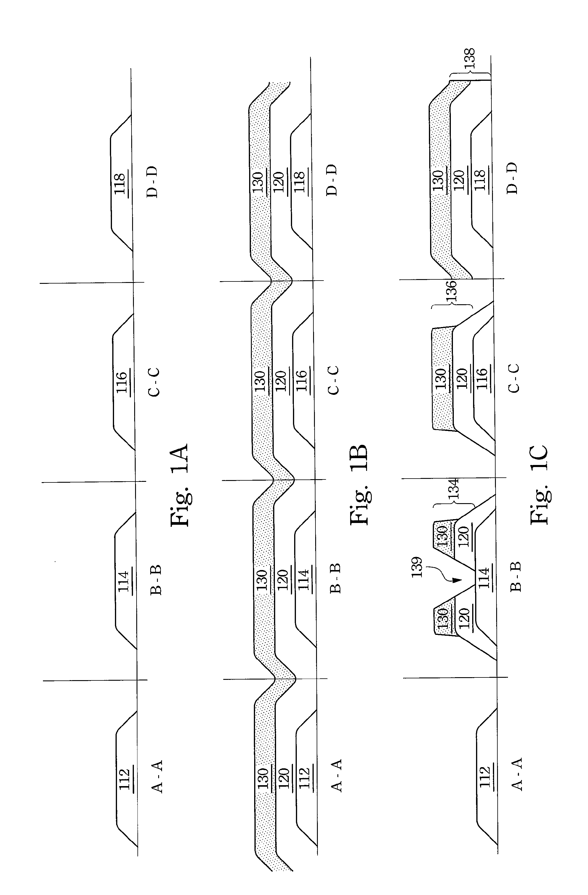
[0021]Please refer to FIG. 1A and FIG. 2A simultaneously. FIG. 1A comprises the A-A cross-sectional view of a scan line, B-B cross-sectional view of a data line, C-C cross-sectional view of a capacitance line and D-D cross-sectional view of a gate electrode in FIG. 2A. At first, a first metal layer is formed on a transparent substrate (not shown in FIG. 1A and FIG. 2A). The first metal layer is defined to form first scan lines 112, first data lines 114, capacitance lines 116 and gate electrodes 118. In FIG. 2A, the first scan lines 112 are parallel to the capacitance lines 116. Both the first scan lines 112 and the capacitance lines 116 have crossing regions 119 respectively. The first data lines 114 are perpendicular to both the first scan lines 112 and the capacitance lines 116. The first data lines 114 are located separately at two sides of the crossing regions 119 of both the first scan lines 112 and the capacitance lines 116. The first data lines 114 don't connect with the cros...
embodiment 2
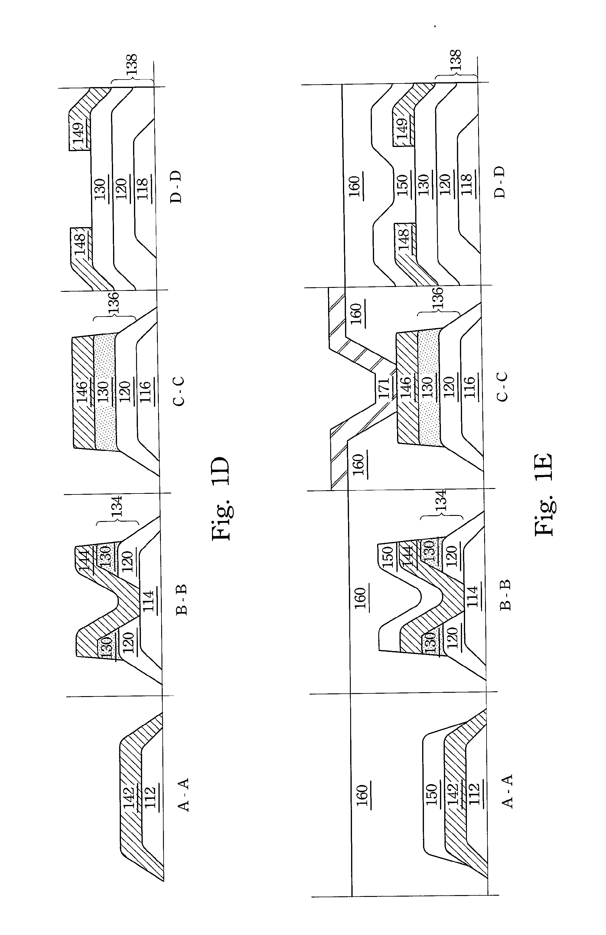
[0030]In embodiment 2, the planarization layer of the embodiment 1 is omitted, so there are some corresponding adjustments on some structures of the LCD array substrate. With the exception of no upper electrodes forming on the capacitance dielectric layer when the second metal layer is defined, all processes from the formation of the first metal layer to the formation of the passivation layer in the embodiment 2 are the same as those in the embodiment 1.
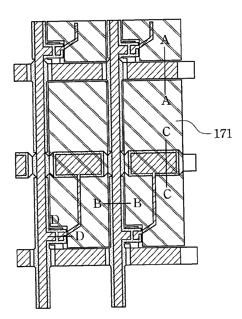
[0031]Please refer to FIG. 3A and FIG. 3B simultaneously. FIG. 3B is the top view of FIG. 3A. After the passivation layer 150 is formed over the substrate, the passivation layer 150 is defined to cover the second scan lines 142, the second data lines 144, the source electrode 148 and the drain electrodes 149. Then, the transparent conducting layer is formed and defined to form the pixel electrodes 171. The pixel electrodes 171 connect with the drain electrodes 149 of the transistors through the connecting points 181.
[0032]When the pa...
embodiment 3
[0034]Because the transparent conducting layer has the property of the conductor, the transparent conducting layer can be used to replace the second metal layer of embodiment 2. Therefore, not only the planarization but also the second metal layer is omitted in embodiment 3. In this embodiment, the transparent conducting layer can be used not only as the pixel electrodes but also as the conductive lines. Moreover, the number of the required masks in the processes is decreased, so that the cost of the processes is decreased. In embodiment 3, all processes from the formation of the first metal layer to the definition of the semiconducting layer and the dielectric layer are the same as those in embodiment 1.
[0035]Please refer to FIG. 4A and FIG. 4B simultaneously. FIG. 4B is the top view of FIG. 4A. After the transparent conducting layer is formed over the substrate, the transparent conducting layer is defined to form the second scan lines 142, the second data lines 144, the source ele...
PUM
 Abstract
Description
Claims
Application Information