
High-power ball grid array package, heat spreader used in the bga package and method for manufacturing the same

a high-power, grid array technology, applied in the field of semiconductor package technology, can solve the problems of difficult mounting of heat spreader on the bga package, inadequacies of bga package for high-power bga package, and inability to apply the conventional package technology to a highly-integrated semiconductor chip having over 400 lead lines, etc., to achieve the effect of reducing the generation of charges, and reducing the generation of defects

Active Publication Date: 2007-11-08
SAMSUNG ELECTRONICS CO LTD
View PDF16 Cites 5 Cited by
  • Summary
  • Abstract
  • Description
  • Claims
  • Application Information

AI Technical Summary

Benefits of technology

The present invention provides a high-power ball grid array package with a heat spreader and a method for manufacturing it. The heat spreader has a ceramic layer and a metal layer with a protection layer, which reduces generation of charges between the semiconductor chip and the heat spreader, thus reducing defects such as electrostatic discharge. The package also includes a passive film to fill the through hole and a matrix solder ball to bond with the semiconductor chip. The printed circuit board has a through hole in its center, with a connection pad and matrix solder balls surrounding it. The heat spreader has a chip supporting body, a lower metal layer, and a protection layer. The method for manufacturing the heat spreader includes preparing an insulating board, forming a metal layer on both surfaces of the insulating board, patterning the metal layer, and forming a protection layer. The ceramic layer is made of AIN, BeO, or Al2O3. The metal layer is made of copper or a copper alloy. The protection layer is made of nickel or a nickel alloy. The method for manufacturing the high-power ball grid array package with the heat spreader reduces generation of charges and improves reliability.

Problems solved by technology

As the number of lead lines increases, a lead frame of the conventional package technology cannot be applied to a highly-integrated semiconductor chip having over 400 lead lines.
However, since a gold wire is formed upwardly to connect the semiconductor chip with the pad of the main body of the package, it is difficult to mount the heat spreader on the BGA package and so such BGA package is not appropriate for a high-power BGA package.
The heat spreader 1110 of such high-power BGA package, however, is composed of conductive copper and surface-processed nickel, a fact which results in a constant voltage between the semiconductor chip 1101 and the heat spreader 1110 during the operation of the semiconductor chip 1101 and can cause damage to the semiconductor chip 1101 in many cases.
The yield of BGA package of the semiconductor device decreases, and the reliability of the semiconductor device may not be ensured when mounting the semiconductor chip on the printed circuit board.

Method used


Image

  • High-power ball grid array package, heat spreader used in the bga package and method for manufacturing the same
  • High-power ball grid array package, heat spreader used in the bga package and method for manufacturing the same
  • High-power ball grid array package, heat spreader used in the bga package and method for manufacturing the same

Examples


Embodiment Construction

[0031] The present invention now will be described more fully with reference to the accompanying drawings, in which preferred embodiments of the invention are shown. In the drawings, the shapes of elements are exaggerated for clarity, and like reference numerals are used to refer to like elements throughout.

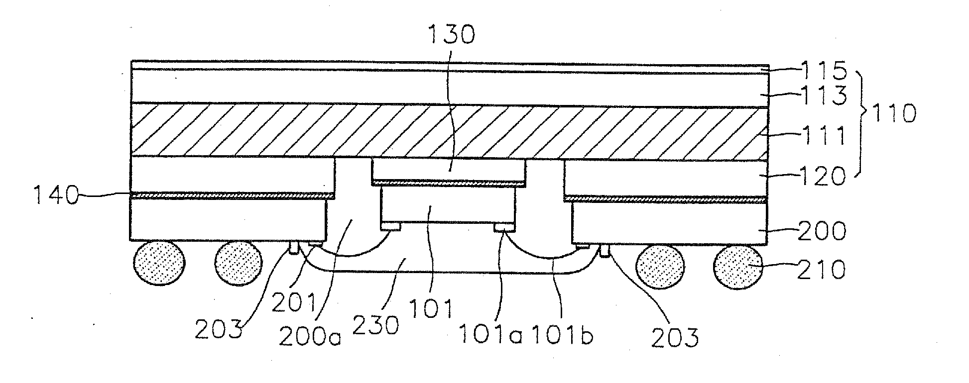
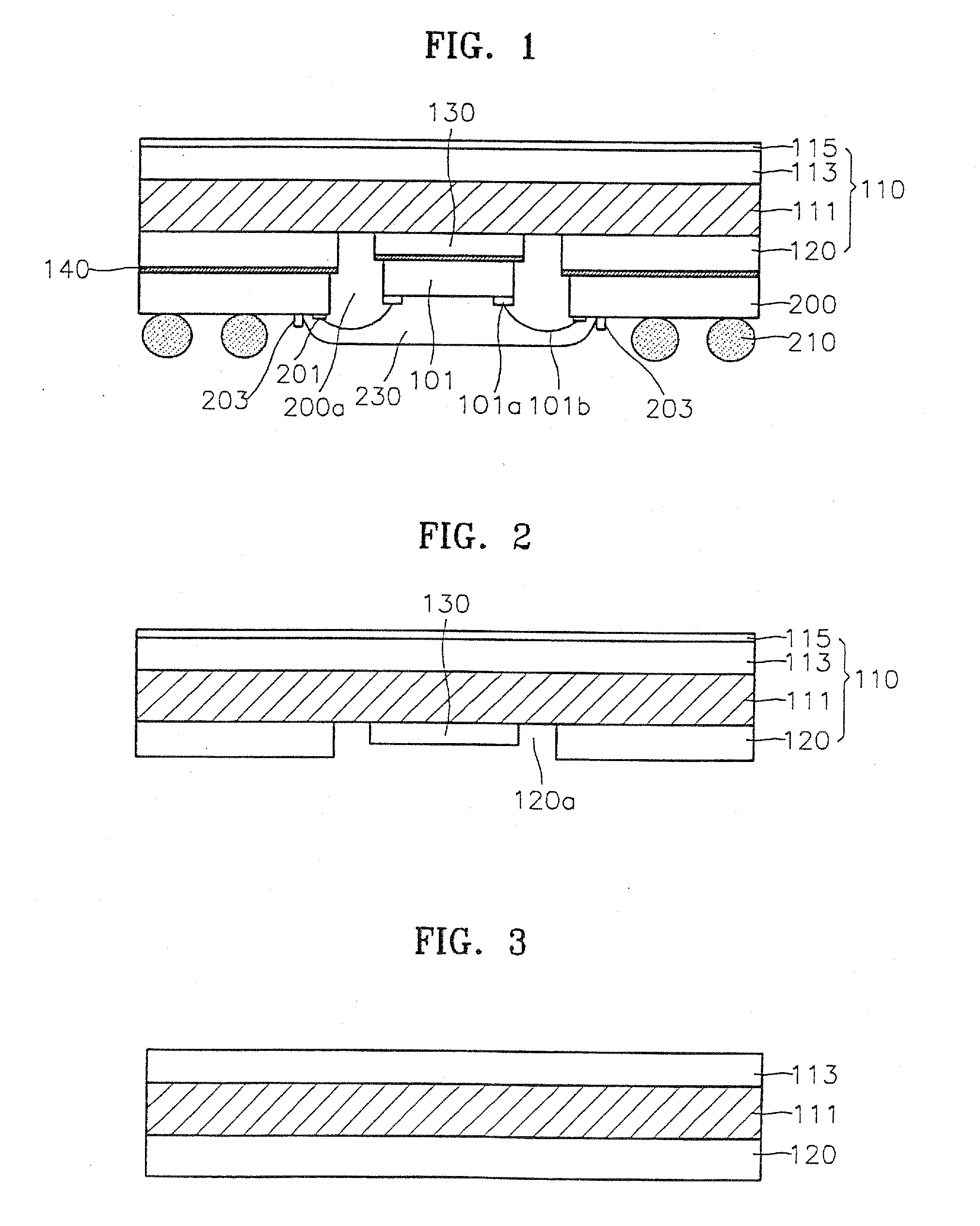
[0032]FIG. 1 is a sectional view of a high-power BGA package of the present invention.

[0033] Referring to FIG. 1, the high-power BGA package of the present invention includes a printed circuit board 200 having a square shape and in which a metal interconnection (not shown) is embedded and a through portion 200a is formed at the center. The printed circuit board 200 includes a connection pad 201 surrounding the through portion 200a, a heat spreader 110 which is attached to a lower metal layer 120 on the surface of the printed circuit board 200 and includes an insulating layer 111 formed of a ceramic material, a semiconductor chip 101 in which a plurality of metal pads 101a at th...


PUM

PropertyMeasurementUnit
thermal conductivityaaaaaaaaaa
poweraaaaaaaaaa
constant voltageaaaaaaaaaa

Abstract

Provided are a high-power ball grid array (BGA) and a method for manufacturing the high-power BGA. The high-power BGA includes a printed circuit board which has a through hole at its center, connection pads which are formed on the bottom of the printed circuit board, matrix solder balls which surround the through hole and are adjacent to the connection pads on the bottom of the printed circuit board, a heat spreader which is formed on the top surface of the printed circuit board and includes an insulating layer of a high thermal conductivity, a semiconductor chip which is mounted downwardly on the bottom surface of the heat spreader, within the through hole, and includes a plurality of pads for bonding via gold wires with the connection pad, and a passive film which fills the through hole and is formed at the bottom of the semiconductor chip. By interposing a ceramic between the semiconductor chip and the heat spreader, for insulating, the generation of charges between the semiconductor chip and the heat spreader can be sharply reduced, and defects such as ESD (electrostatic discharge) can be reduced when testing for the ESD and mounting the package.

Description

CROSS REFERENCE TO RELATED APPLICATIONS [0001] This application is a divisional of U.S. patent application Ser. No. 10 / 459,400, filed Jun. 10, 2003, now pending, which is claims priority from Korean Patent Application No. 2002-32972, filed on Jun. 12, 2002, the disclosure of which are incorporated herein in its entirety by reference.BACKGROUND OF THE INVENTION [0002] 1. Field of the Invention [0003] The present invention relates to semiconductor packages and, more particularly, to a high-power ball grid array (BGA) package having a heat spreader, a method for manufacturing the heat spreader, a BGA printed circuit board (PCB) to which the method is applied, and a method for manufacturing the BGA PCB. [0004] 2. Description of the Related Art [0005] As devices become highly integrated, the number of connection pads in a semiconductor device such as a semiconductor memory device increases. Thus, the number of lead lines in a package included in a PCB also increases. As the number of lea...

Claims


Application Information

Patent Timeline
Patent Type & Authority Applications(United States)
IPC IPC(8): H05K7/20H01L23/15H01L23/12H01L23/24H01L23/31H01L23/36H01L23/373
CPCH01L23/24Y10T29/49156H01L23/36H01L2224/48091H01L2224/73265H01L2224/92247H01L2924/01078H01L2924/01079H01L2924/15153H01L2924/1517H01L2924/15311H01L2924/1532H01L23/3128H01L2224/45144H01L2924/01322H01L24/48H01L2924/00014H01L2924/00H01L2924/12042H01L24/45H01L2924/181H01L2924/00015H01L2924/00012
Inventor KWON, HEUNG-KYUCHO, TAE-JEKIM, MIN-HA
Owner SAMSUNG ELECTRONICS CO LTD
Learn More