Organic semiconductor crystalline film, method for preparing the same, organic transistor, and organic phototransistor

Active Publication Date: 2007-11-15
CHANGCHUN INST APPLIED CHEM CHINESE ACADER +1
View PDF25 Cites 18 Cited by
  • Summary
  • Abstract
  • Description
  • Claims
  • Application Information

AI Technical Summary

Benefits of technology

[0009]In order to overcome the deficiency of the prior art, an organic semiconductor crystalline film is provided in the present invention. The organic semiconductor crystalline film of the present invention is characterized in that organic semiconductor molecules in the organic semiconductor crystalline film are arrange

Problems solved by technology

Because there is no oriented relationship between the organic film prepared by vapor phase deposition method and the substrate, the grain boundary defects can not be controlled effectively, and therefore the carrier mobility of thus prepared organic semiconductor polycrystalline film is lower

Method used


Image

  • Organic semiconductor crystalline film, method for preparing the same, organic transistor, and organic phototransistor
  • Organic semiconductor crystalline film, method for preparing the same, organic transistor, and organic phototransistor
  • Organic semiconductor crystalline film, method for preparing the same, organic transistor, and organic phototransistor

Examples


example 1

[0078]Target materials of Ta2O5, Al2O3, TiO2, and SiO2 used in the present invention were all commercial products, which were employed directly. Glass substrates and plastic substrates were commercial products, and were employed after washing. 6P, ZnPc, and F16CuPc used herein were commercial products which were employed after being purified by sublimation method.

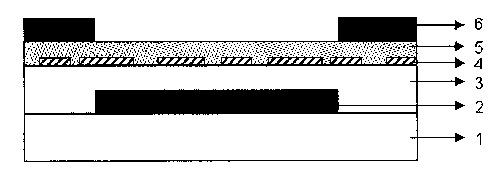
[0079]A layer of Ta2O5, Al2O3, TiO2, or SiO2 film having a thickness of 150-500 nm was formed on a glass substrate or plastic substrate 1 by sputtering continuously using radio-frequency magnetron sputtering method. Thereafter, an organic semiconductor 6P ordered molecular layer 4 having a thickness of 5-20 nm was deposited on the Ta2O5, Al2O3, TiO2, or SiO2 film at a growth temperature of 30-180° C. using molecular vapor phase deposition method, thus an ordered substrate was constituted, under a vacuum degree of 10−4 Pa. Thereafter, an organic semiconductor ZnPc or F16CuPc crystalline film 5 having a thickness of 5-20 nm w...

example 2

[0083]A layer of Ta2O5, Al2O3, TiO2, or SiO2 film having a thickness of 150-500 nm was formed on a glass substrate or plastic substrate 1 by sputtering continuously using radio-frequency magnetron sputtering method. Thereafter, an organic semiconductor 6P ordered molecular layer 4 having a thickness of 5-20 nm was deposited on the Ta2O5, Al2O3, TiO2, or SiO2 film at a growth temperature of 30-180° C. using molecular vapor phase deposition method, thus an ordered substrate was constituted, under a vacuum degree of 10−4 Pa. Thereafter, an organic semiconductor ZnPc or F16CuPc crystalline film 5 having a thickness of 5-50 nm was deposited continuously at a growth temperature within 30-200° C. on the ordered substrate. The other conditions and results were the same as those of Example 1.

example 3

[0084]A layer of Ta2O5, Al2O3, TiO2, or SiO2 film having a thickness of 250 nm was formed on a glass substrate or plastic substrate 1 by sputtering continuously using radio-frequency magnetron sputtering method. Thereafter, an organic semiconductor 6P ordered molecular layer 4 having a thickness of 10 nm was deposited on the Ta2O5, Al2O3, TiO2, or SiO2 film at a growth temperature of 90° C. using molecular vapor phase deposition method, thus an ordered substrate was constituted, under a vacuum degree of 10−4 Pa. Thereafter, an organic semiconductor ZnPc or F16CuPc crystalline film 5 having a thickness of 20 nm was deposited continuously at a growth temperature of 50° C. on the ordered substrate. The other conditions and results were same as those of Example 1.


PUM


Abstract

An organic semiconductor crystalline film and weak oriented epitaxy growth preparation method thereof. The organic semiconductor crystalline film is a n-type semiconductor or a p-type semiconductor, and organic semiconductor crystal molecules in the organic semiconductor crystalline film are oriented in a stand-up manner on the ordered substrate, and have an oriented relationship with the ordered substrate. The organic semiconductor crystalline film prepared by the present invention is useful for organic transistor and organic phototransistor devices. The method of the present invention can control the high carrier mobility direction of organic semiconductor crystals to have ordered orientation in the film, enhance contacts between crystals, improve mechanical strength and micro-machining property of the film, and give a high carrier mobility. The carrier mobility of weak oriented epitaxially grown film of the present invention is 0.32 cm2/Vs, which is 5 times as large as that of a vapor phase deposited film, and is similar to that of single crystal. The present invention is adapted to glass substrates and plastic substrates.

Description

BACKGROUND OF THE INVENTION[0001]1. Cross Related Applications[0002]This application claims priority from Chinese Patent Application Serial No. 200610016822.4 filed Apr. 29, 2006.[0003]2. Field of the Invention[0004]The present invention relates to an organic semiconductor crystalline film, a weak oriented epitaxy growth preparation method for preparing the same, and an organic film electronic device such as organic transistor and organic phototransistor comprising the organic crystalline film prepared by the weak oriented epitaxy growth method.BACKGROUND ART[0005]In recent years, organic semiconductor materials with high carrier mobility properties and exhibit great potential in the markets of information displays, integrated circuits, photovoltaic cells and sensors. The high carrier mobility property is mainly reflected by organic semiconductor single crystal. The “Physical Vapor Growth” for preparing an organic semiconductor single crystal was reported firstly by Kloc et al., Jou...

Claims


Application Information

Patent Timeline
IPC IPC(8): H01L29/08H01L35/24H01L51/00
CPCH01L51/0012H01L51/0068Y02E10/549H01L51/0545H01L51/428H01L51/0078H10K71/191H10K85/655H10K85/311H10K10/466H10K30/65
Inventor YAN, DONGHANGWANG, HAIBOZHU, FENGSHI, JIANWUSONG, DE
Owner CHANGCHUN INST APPLIED CHEM CHINESE ACADER
Why Eureka
Try Eureka