

Method of manufacturing nonvolatile memory device
- Summary
- Abstract
- Description
- Claims
- Application Information
AI Technical Summary
Benefits of technology
Problems solved by technology
Method used
Image

Examples
example 1
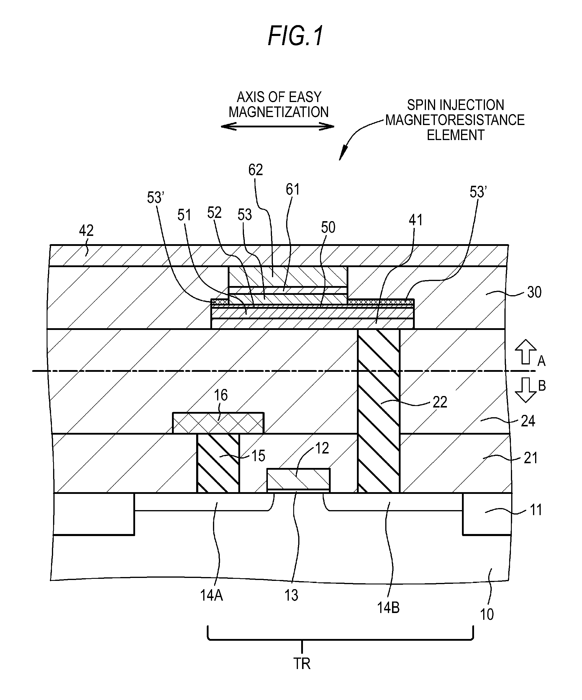
[0066]Example 1 relates to a method of manufacturing a nonvolatile memory device according to the first embodiment of the invention. FIG. 1 is a schematic partial sectional view of the nonvolatile memory device of the first embodiment obtained according to a method of manufacturing a nonvolatile memory device of example 1.
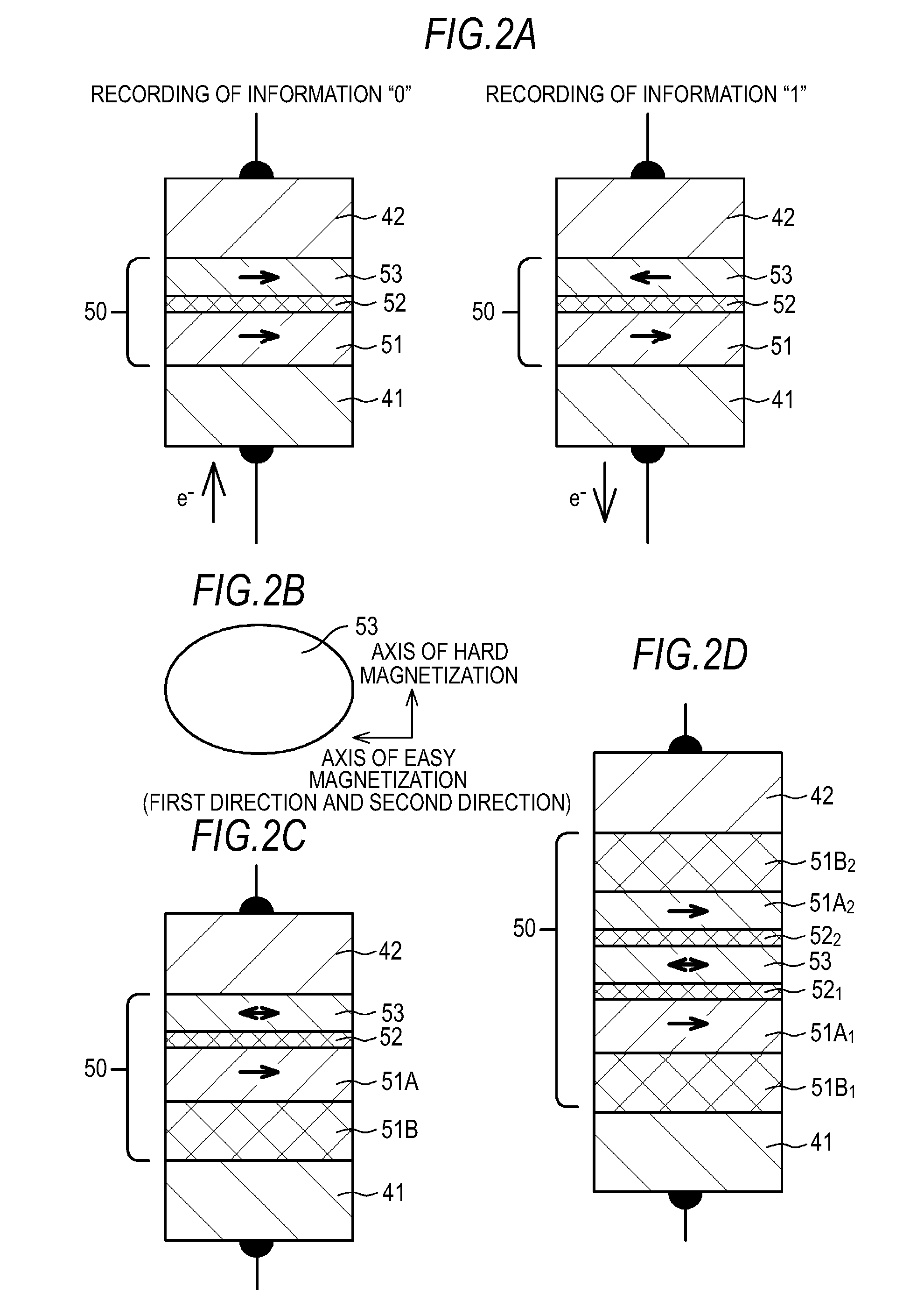
[0067]The nonvolatile memory device of example 1 or example 2, which will be described later, is a nonvolatile memory device having a laminated structure 50 in which a first magnetic material layer 51, a tunnel insulator film 52, and a second magnetic material layer 53 are sequentially laminated, and information is recorded therein when an electric resistance value changes depending on the magnetic reversal state. The nonvolatile memory device of example 1 or example 2, which will be described later, further has a first wiring line 41 electrically connected to a lower part of the laminated structure 50, and a second wiring line 42 electrically connected to an upper...
example 2
[0150]Example 2 is a modification of example 1. In example 1, the nonvolatile memory device of the first embodiment is the spin injection magnetoresistance effect device of in-plane magnetization system. On the other hand, in example 2, the device is a spin injection magnetoresistance effect device of perpendicular magnetization system. In example 2, the planar shape of the region of the second magnetic material layer (recording layer) that has not been oxidized is circle in view of securement of workability and uniformity of the direction of the axis of easy magnetization in the second magnetic material layer (recording layer).
[0151]Specifically, the configuration of the laminated structure is as below.
Second Magnetic Material Layer (Recording Layer)
[0152]A laminated structure of a CoFeB layer having a thickness of about 1 nm and a TbFeCo layer having a thickness of about 3 nm
Tunnel Insulator Film
[0153]An Mgo film having a thickness of 1.0 nm
First Magnetic Material Layer (Magnetiza...
example 3
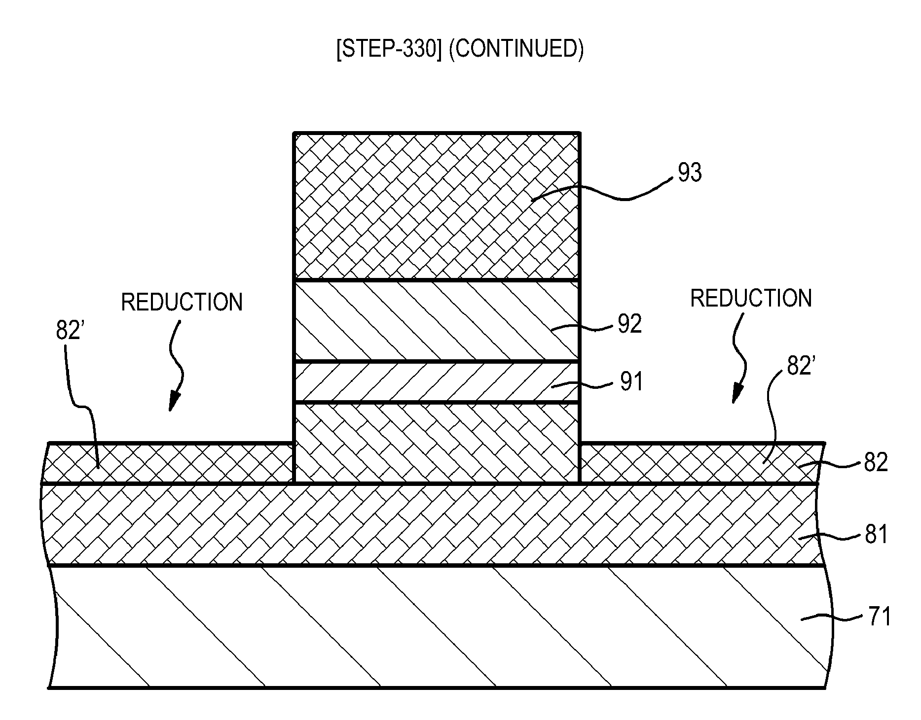
[0164]Example 3 relates to a method of manufacturing a nonvolatile memory device according to the second embodiment of the invention. FIG. 7A conceptually shows a sectional structure of a resistance change layer in the nonvolatile memory device of the second embodiment obtained in the method of manufacturing the nonvolatile memory device of example 3, and FIG. 7B shows an equivalent circuit diagram. In the nonvolatile memory device of example 3, a resistance change layer 80 includes an ion conductor containing a metal. Further, in the nonvolatile memory device of example 3, a selection transistor TR is provided. Note that the configuration, structure of the selection transistor in the nonvolatile memory device of example 3 maybe made the same as the configuration, structure of the nonvolatile memory device of example 1, and the arrangement relation between the nonvolatile memory device of example 3 and the selection transistor maybe made the same as the arrangement relation between ...
PUM
 Abstract
Description
Claims
Application Information