

Semiconductor device manufacturing apparatus and method of using the same
a technology of semiconductor devices and manufacturing apparatuses, which is applied in the direction of coatings, chemical vapor deposition coatings, coatings, etc., can solve the problems of contaminating the process apparatus, contaminating the semiconductor substrate, and damaging the plasma generated in the process chamber
- Summary
- Abstract
- Description
- Claims
- Application Information
AI Technical Summary
Benefits of technology
Problems solved by technology
Method used
Image

Examples
Embodiment Construction
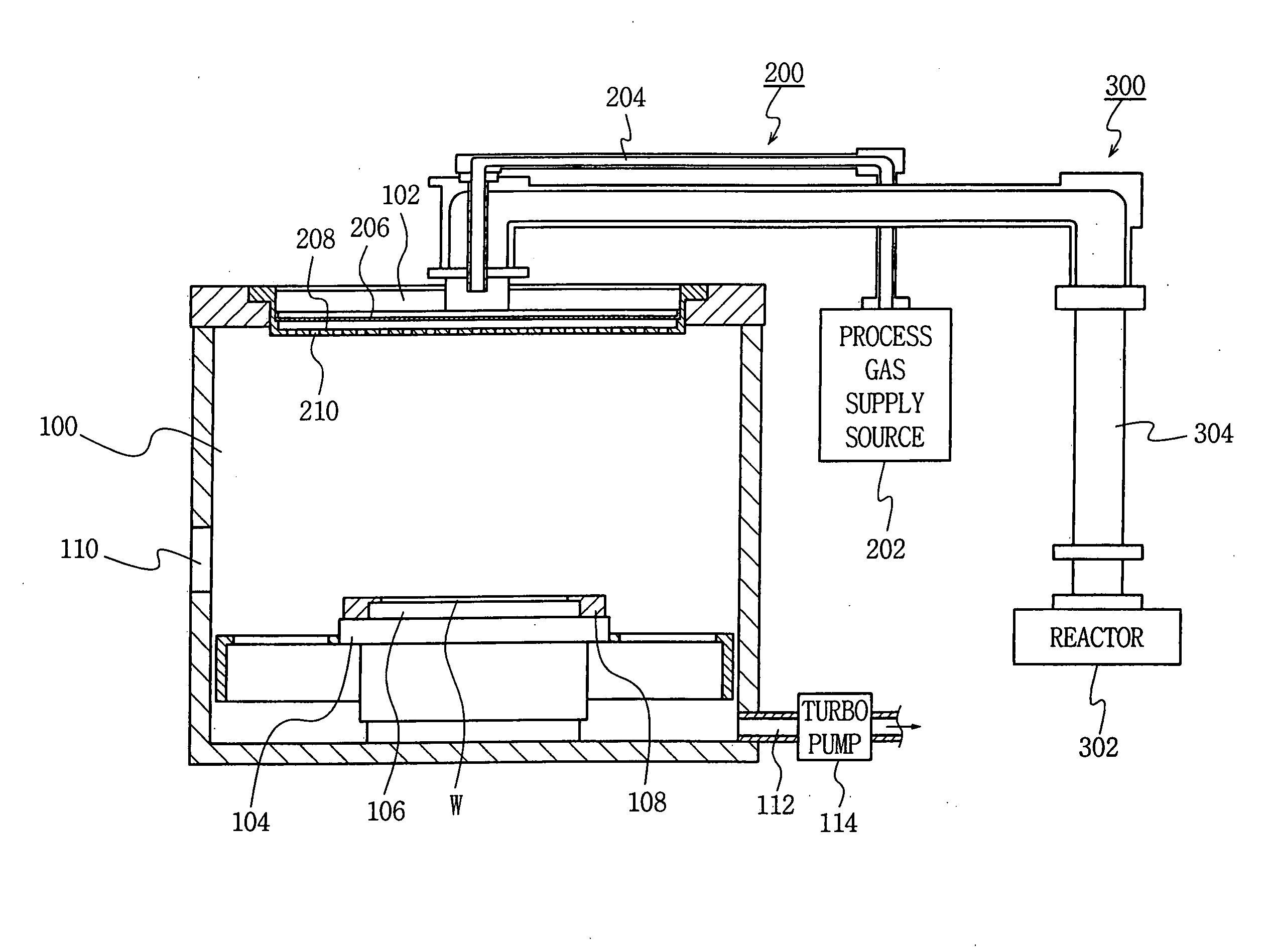
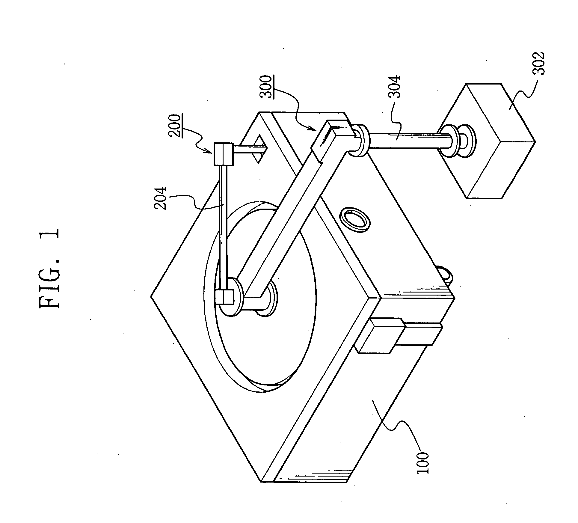
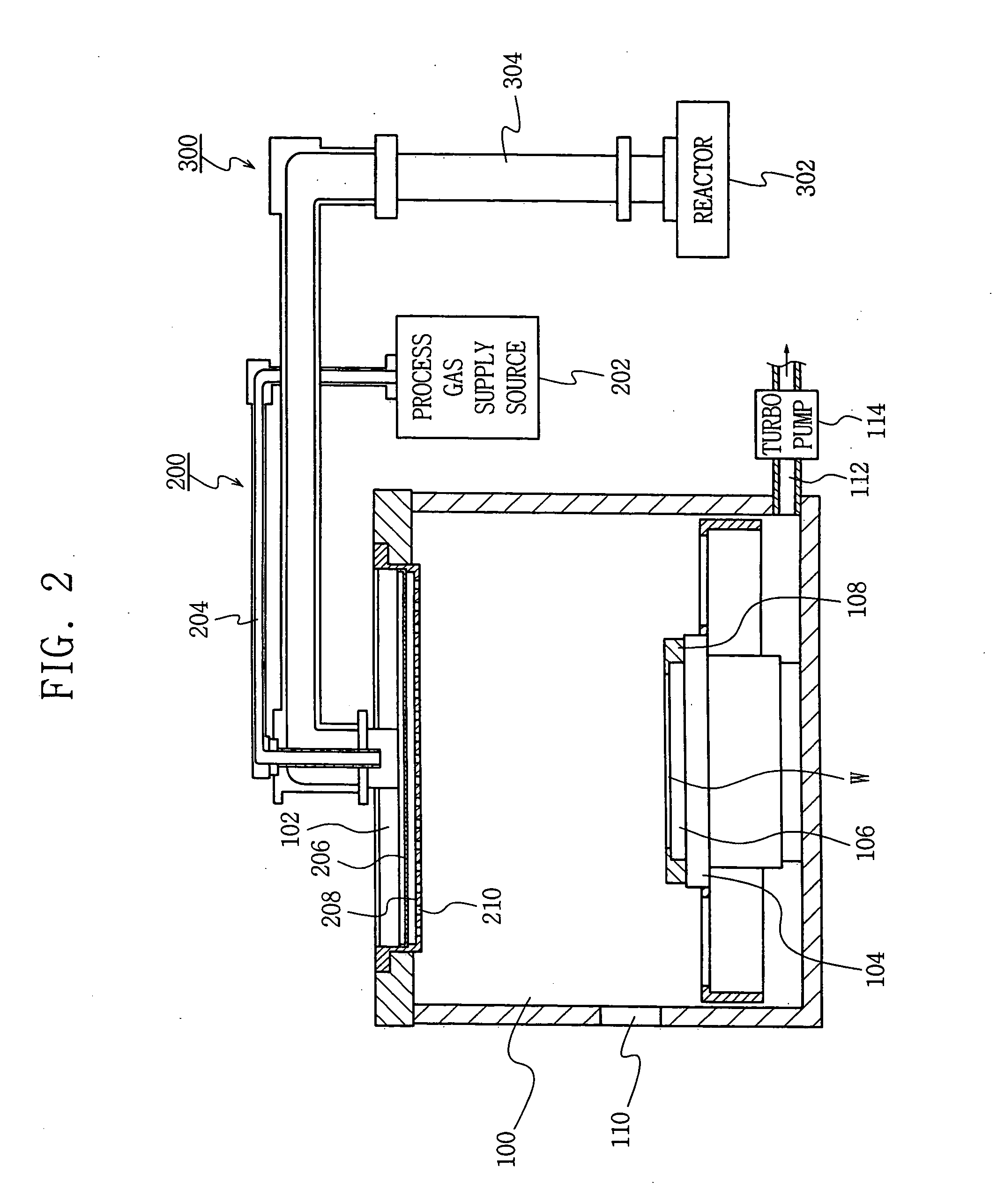
[0025]FIGS. 1 and 2 illustrate a thin layer deposition apparatus as one example of a semiconductor device manufacturing apparatus according to the present invention. More specifically, FIGS. 1 and 2 illustrate a plasma-enhanced chemical vapor deposition (CVD) apparatus for forming a plasma-enhanced tetraethoxysilane (PETEOS) insulating layer on a substrate. However, although the present invention will be described in the context of a plasma-enhanced chemical vapor deposition (CVD) apparatus, the present invention may be applied to other processing apparatus. For instance, the present invention can be applied to etching and diffusion apparatus.
[0026]Referring first to FIG. 1, the plasma-enhanced chemical vapor deposition (CVD) apparatus has a process chamber 100 in which a process of forming a PETEOS insulating layer on a substrate is performed. A process gas supply unit 200 is coupled to a lid of the process chamber 100. The process gas supply unit 200 supplies the process gas, used...
PUM
 Abstract
Description
Claims
Application Information