

Semi-transmissive type liquid-crystal display device and method of fabricating the same
- Summary
- Abstract
- Description
- Claims
- Application Information
AI Technical Summary
Benefits of technology
Problems solved by technology
Method used
Image

Examples
first embodiment
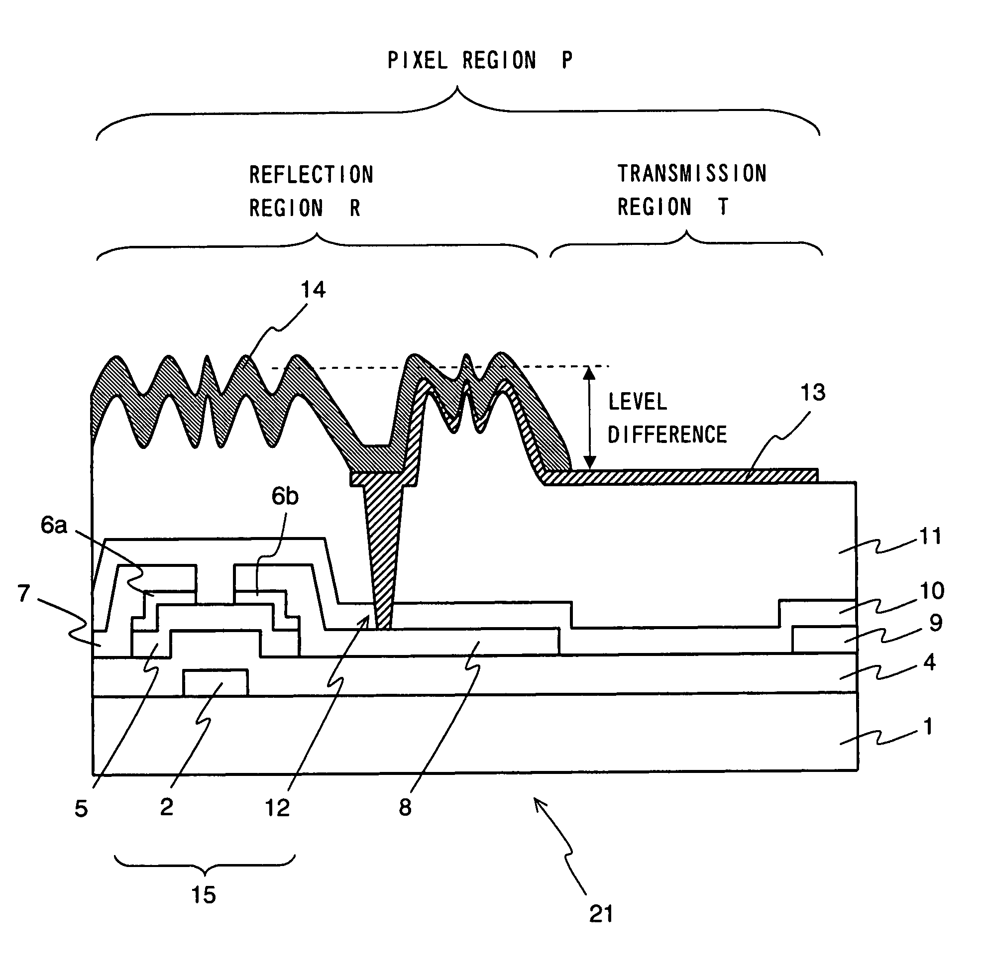
[0094]The schematic structure of the TFT array substrate used for a semi-transmissive type LCD device according to a first embodiment of the invention is shown in FIG. 3, and the cross-sectional structure thereof along the line IV-IV in FIG. 3 is shown in FIG. 4. The cross-sectional structure of the LCD device itself along the line IV-IV is shown in FIG. 5. These figures show the pixel structure of one of the pixel regions P arranged in a matrix array.
[0095]As shown in FIG. 3, with the TFT array substrate 21 used for the LCD device according to the first embodiment of the Invention, the pixel region P corresponding to one pixel is one of the rectangular regions defined by gate lines 3 extending along the horizontal direction of FIG. 3 and data lines 9 extending along the vertical direction thereof. The pixel region P is divided into a transmission region T and a reflection region R, where a transmission electrode 13 is formed in the transmission region T and a reflection electrode 1...
second embodiment
[0141]FIGS. 14 to 15 are partial cross-sectional views along the line IV-IV in FIG. 3, which show the fabrication process steps of the TFT array substrate used for a semi-transmissive type LCD device according to a second embodiment of the invention, respectively. Each of these figures relates to one of the pixel regions P.
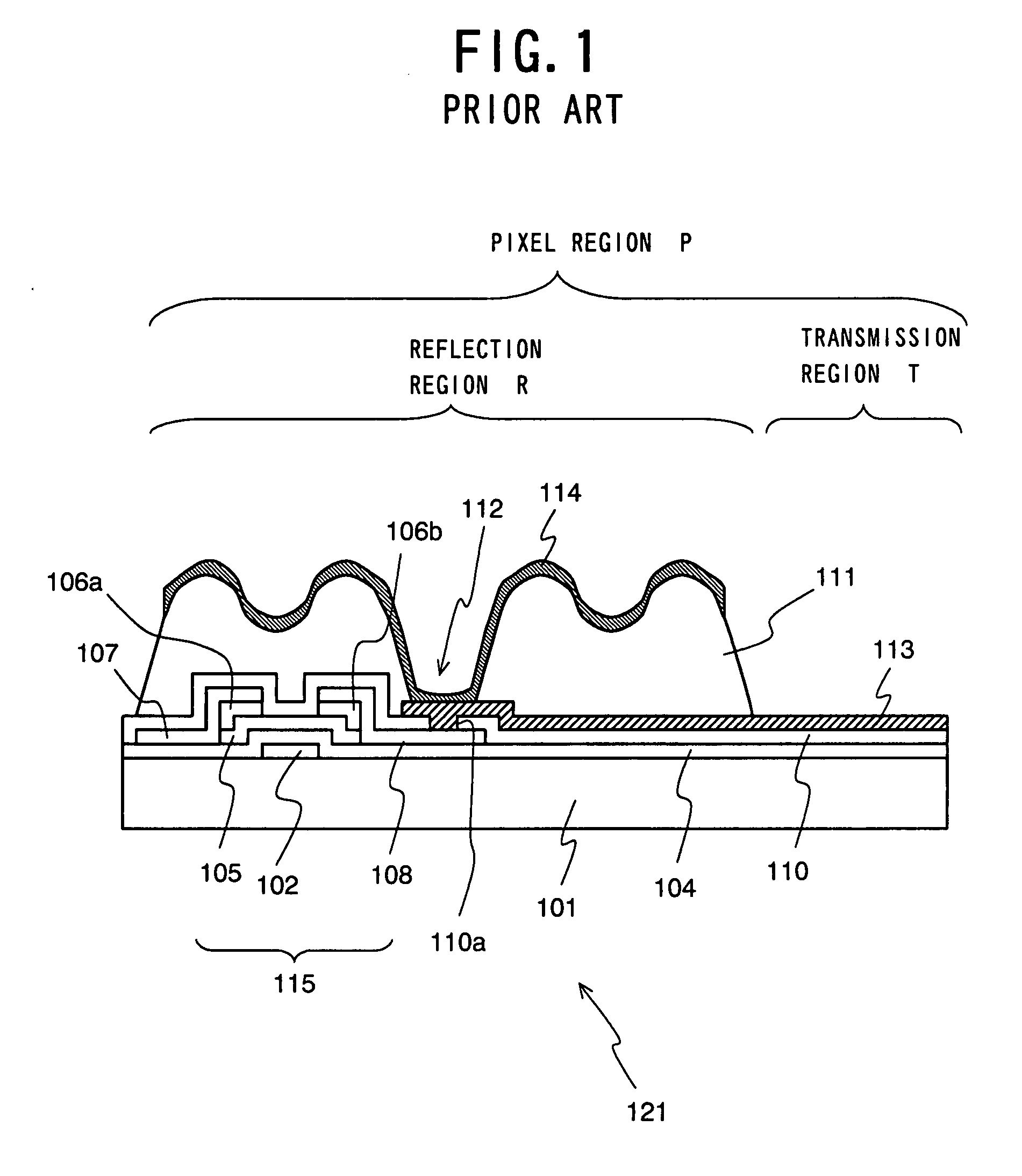
[0142]With the method of fabricating the semi-transmissive type LCD device according to the first embodiment of the invention, as explained above, the interlayer insulating film 11 is exposed through the first to third exposure steps. This means that the exposure steps are carried out three times while changing the photomasks. Unlike this, with the method of fabricating the LCD device according to the second embodiment, the count of the necessary exposure steps can be decreased to two.
[0143]First, in the same manner as that of the first embodiment, a photosensitive acrylic resin film as the interlayer insulating film 11 is formed on the passivation film 10 by a sp...
third embodiment
[0156]FIGS. 16 to 17 are partial cross-sectional views along the line IV-IV in FIG. 3, which show the fabrication process steps of the TFT array substrate used for a semi-transmissive type LCD device according to a third embodiment of the invention, respectively. Each of these figures relates to one of the pixel regions P.
[0157]In the method of fabricating the device of the third embodiment also, the count of the above-described necessary exposure steps can be reduced to two.
[0158]First, in the same manner as that of the first embodiment, a photosensitive acrylic resin film as the interlayer insulating film 11 is formed on the passivation film 10 by a spin-coating method, thereby forming the structure of FIG. 7.
[0159]Next, using the first photomask 16 used in the first exposure step in the first embodiment (see FIG. 8), predetermined UV light is irradiated to the acrylic resin film, i.e., the interlayer insulating film 11, thereby selectively exposing the film 11 (the first exposure...
PUM
 Abstract
Description
Claims
Application Information