

Rolling mold for microstructured film imprinting
a microstructured film and mold technology, applied in the field of imprint technology, can solve the problems of microstructure damage, difficult fabrication of integrated circuits of a smaller size, restricted integration circuit fabrication, etc., and achieve the effects of high hardness, simple and easy operation, and flexible position adjustmen
- Summary
- Abstract
- Description
- Claims
- Application Information
AI Technical Summary
Benefits of technology
Problems solved by technology
Method used
Image

Examples
first embodiment
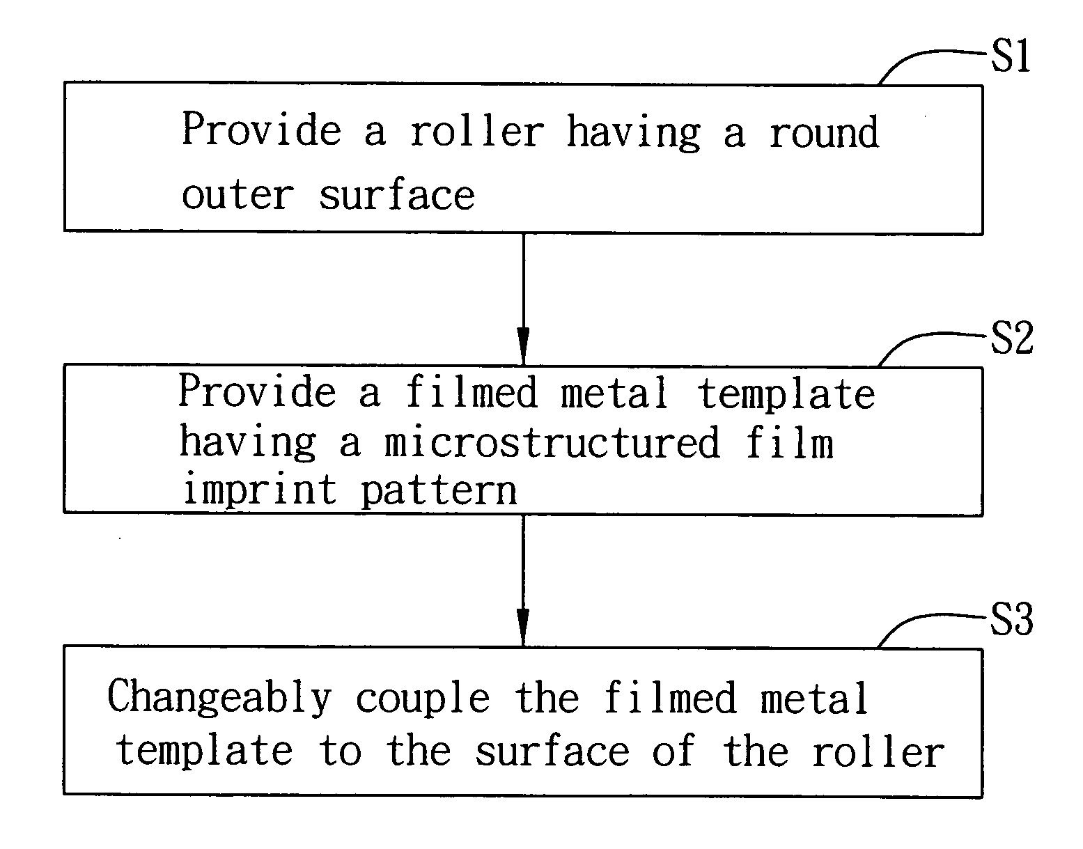
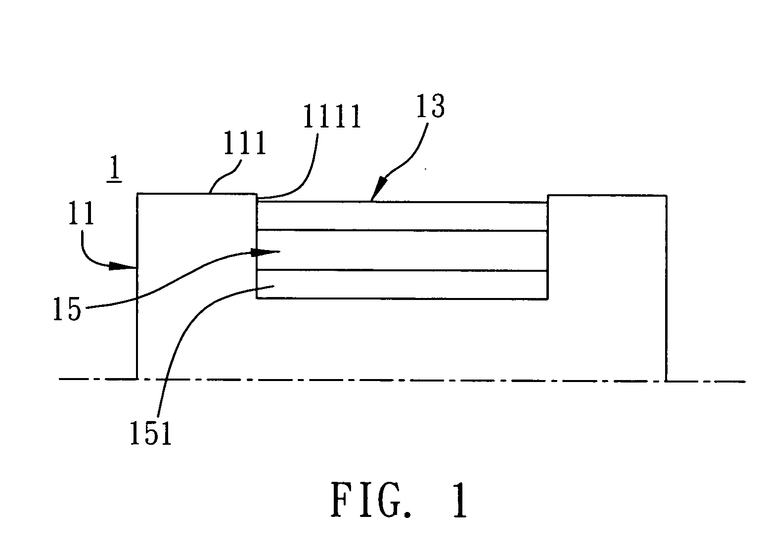
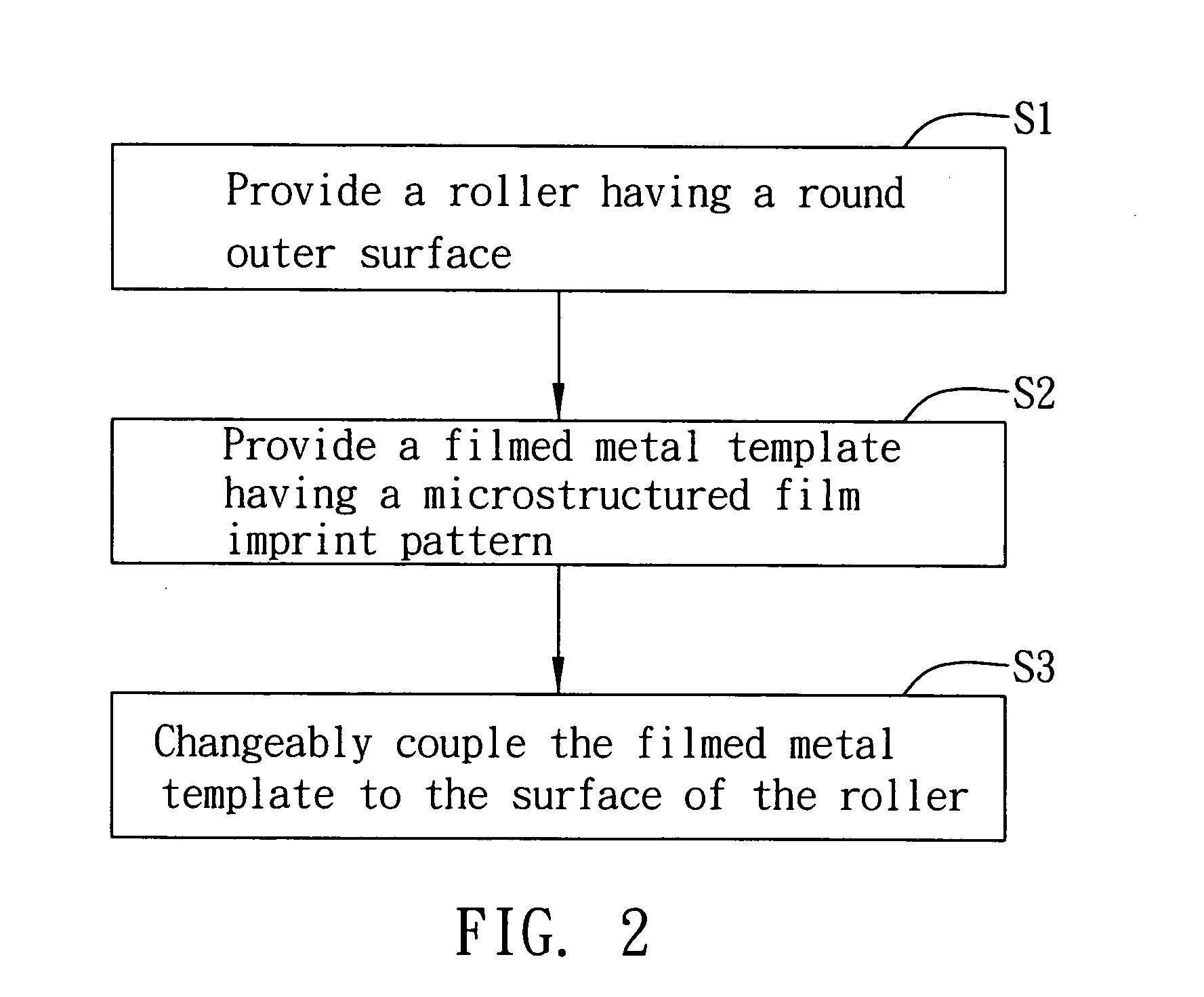
[0027]Referring to FIGS. 1 and 2 for the schematic views of a rolling mold for microstructured film imprinting according to a first preferred embodiment of the invention, a rolling mold for microstructured film imprinting 1 comprises a roller 11, a filmed metal template 13 coupled to the roller 11, and a magnetic substance 15 disposed between the roller 11 and the filmed metal template 13.
[0028]The roller 11 has a round outer surface 111, and the round outer surface 111 has an appropriate round outer tolerance to allow the magnetic substance 15 to be embeddedly attached to the round outer surface 111. In this embodiment, the roller 11 is a non-metal roller, and the round outer surface 111 of the roller 11 has a template containing portion 1111 such as a groove. It is noteworthy that the template containing portion 1111 of this embodiment surrounds the round outer surface 111 completely, but it is not limited to such arrangement. The template containing portion 1111 can also be insta...
second embodiment
[0035]Referring to FIG. 3, which are schematic views of a second preferred embodiment of the present invention, elements identical or similar to those described in the foregoing embodiment are represented by the symbols of identical or similar elements, and the related detailed description is herein omitted for brevity.
[0036]The most significant differences between the second preferred embodiment and the first preferred embodiment are as follows: the roller of the first embodiment is a non-metal roller, but the roller of the second embodiment is a metal roller; and the filmed metal template of the first embodiment is disposed at the template containing portion on the roller round outer surface of the roller, and the filmed metal template of the second embodiment is disposed on the round outer surface of the roller.
[0037]Referring to FIG. 3, the magnetic substance 15 is embedded into a portion of a round outer surface 111 of the roller 11, and the magnetic substance 15 is a magnetic ...
third embodiment
[0038]Referring to FIG. 4, which is a schematic view of a third preferred embodiment of the present invention, elements identical or similar to those described in the foregoing embodiment are represented by the symbols of identical or similar elements, and the related detailed description is herein omitted for brevity.
[0039]The most significant difference between the roller of the third embodiment and the roller of the foregoing embodiments resides in that the roller of the third embodiment is a roller made of a magnetically permeable material.
[0040]Referring to FIG. 4, the roller 11 is a roller made of a magnetically permeable material, and thus the glue 151 used in the first embodiment can be omitted, and the roller 11 can be coupled directly to the magnetic substance 15, and the magnetic force of the magnetic substance 15 can couple the filmed metal template 13 to the roller 11 at the same time.
[0041]From the second and third embodiments, the glue used in the first embodiment for...
PUM
| Property | Measurement | Unit |
|---|---|---|
| thickness | aaaaa | aaaaa |
| size | aaaaa | aaaaa |
| microstructured | aaaaa | aaaaa |
Abstract
Description
Claims
Application Information