Thin film transistor, array substrate having the thin film transistor and method of manufacturing the array substrate

Inactive Publication Date: 2007-11-29
SAMSUNG ELECTRONICS CO LTD
View PDF4 Cites 5 Cited by
  • Summary
  • Abstract
  • Description
  • Claims
  • Application Information

AI Technical Summary

Benefits of technology

[0010]Embodiments of the present invention provide a thin film transistor capable of enhancing electric properties by preventing patterning errors, an array substrate having the above thin film transistor, and a method of manufacturing the above array substrate.
[0018]According to exemplary embodiments of the present invention, an acute angle between a gate electrode and a grain boundary prevents grain boundaries from being formed at a boundary between a channel part and an ion doped part. As a result, electrical mobility of a semiconductor layer is enhanced.

Problems solved by technology

Thus, the grain boundaries can deteriorate electrical properties, for example, such as electrical mobility.

Method used


Image

  • Thin film transistor, array substrate having the thin film transistor and method of manufacturing the array substrate
  • Thin film transistor, array substrate having the thin film transistor and method of manufacturing the array substrate
  • Thin film transistor, array substrate having the thin film transistor and method of manufacturing the array substrate

Examples


Embodiment Construction

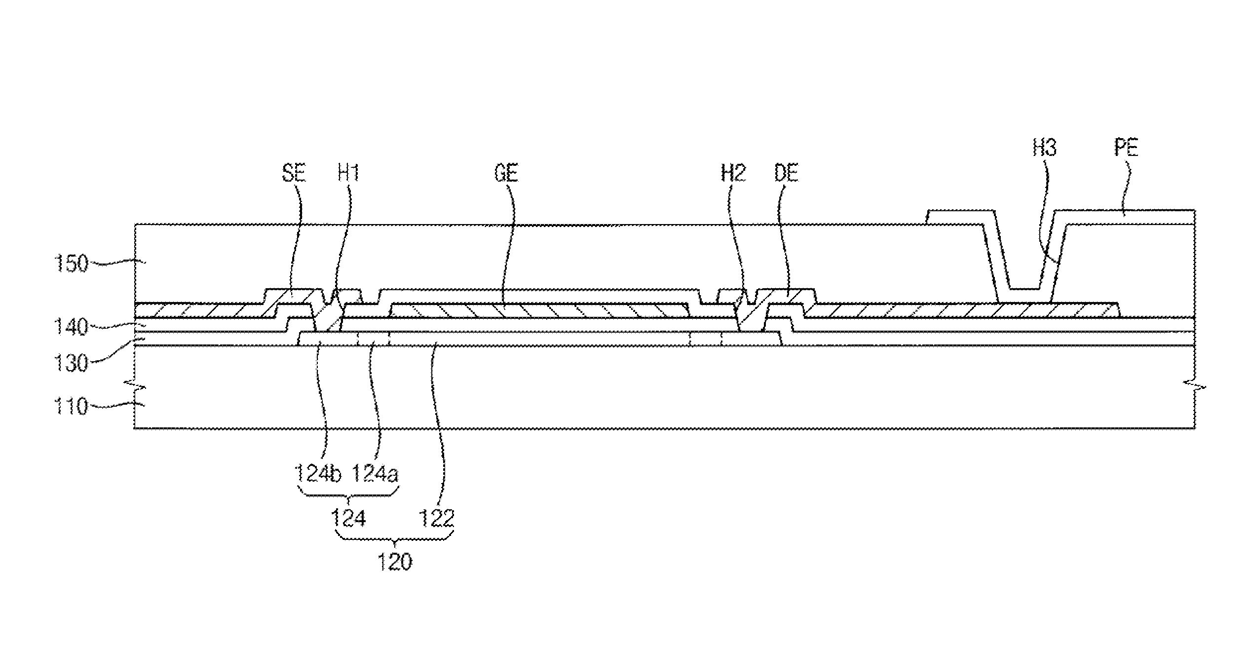
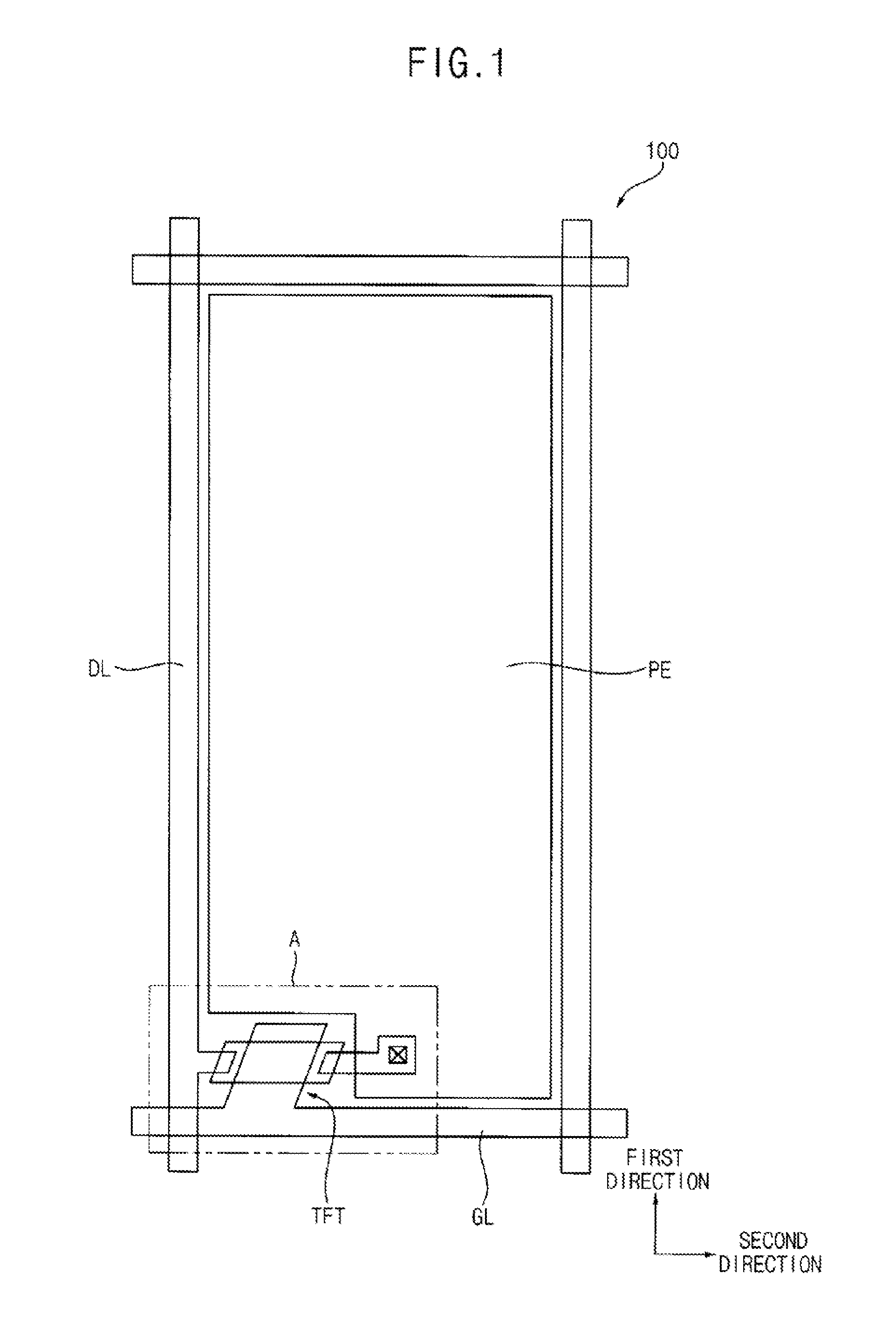
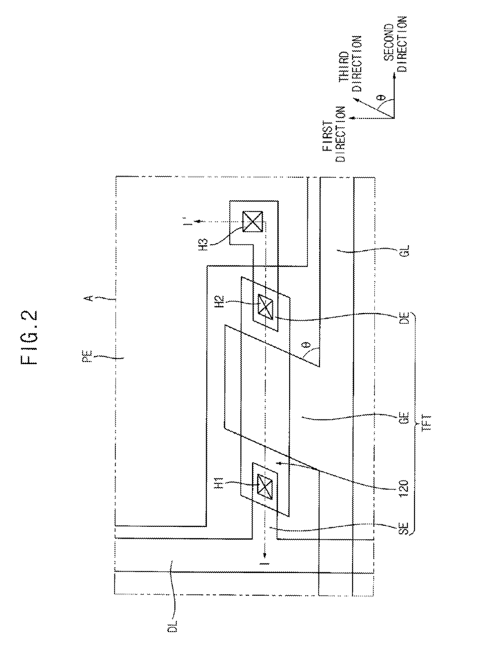
[0031]Exemplary embodiments of the invention are described more fully hereinafter with reference to the accompanying drawings. This invention may, however, be embodied in many different forms and should not be construed as limited to the embodiments set forth herein.

[0032]In an embodiment, a display panel includes an array substrate, an opposite substrate and a liquid crystal layer.

[0033]The array substrate includes a plurality of pixel electrodes, thin film transistors and signal lines. The pixel electrodes are disposed in a matrix. The thin film transistors apply driving voltages to the pixel electrodes, respectively. The signal lines provide signal voltages to the thin film transistors, respectively.

[0034]The opposite substrate faces the array substrate. The opposite substrate may include a transparent and conductive common electrode and color filters. The color filters are disposed at a position corresponding to the pixel electrodes, respectively. For example, the color filters ...


PUM


Abstract

A thin film transistor includes a semiconductor layer a source electrodes a drain electrode and a gate electrode. The semiconductor layer includes a plurality of grain boundaries disposed along a first direction. An acute angle between a gate electrode and a grain boundary prevents grain to boundaries from being formed at the boundary between a channel part and an ion doped part.

Description

CROSS-REFERENCE TO RELATED APPLICATION[0001]This application claims priority to Korean Patent Application No. 2006-47405 filed on May 26, 2006, the disclosure of which is incorporated by reference in its entirety.BACKGROUND OF THE INVENTION[0002]1. Technical Field[0003]The present invention relates to a thin film transistor, an array substrate having the thin film transistor and a method of manufacturing the array substrate, and more particularly, to a thin film transistor having enhanced electrical properties.[0004]2. Discussion of the Related Art[0005]An amorphous silicon (a-Si) thin film transistor may be used as a switching device of a liquid crystal display (LCD). A polysilicon (poly-Si) thin film transistor having a relatively faster operating speed may be more likely used in a liquid crystal display (LCD) of mobile devices to reduce the manufacturing cost and to obtain a highly fine structure by directly integrating circuits on a substrate. For example, in an organic light em...

Claims


Application Information

Patent Timeline
IPC IPC(8): H01L29/04H01L21/84
CPCH01L27/1296H01L29/04H01L29/78675H01L29/66757H01L29/42384
Inventor PARK, JI-YONGKIM, DONG-BYUMKIM, JUNG-HYUNYI, CHUNG
Owner SAMSUNG ELECTRONICS CO LTD
Why Eureka
Try Eureka