
Semiconductor device manufacturing method

Active Publication Date: 2007-11-29
GK BRIDGE 1
View PDF16 Cites 1 Cited by
  • Summary
  • Abstract
  • Description
  • Claims
  • Application Information

AI Technical Summary

Benefits of technology

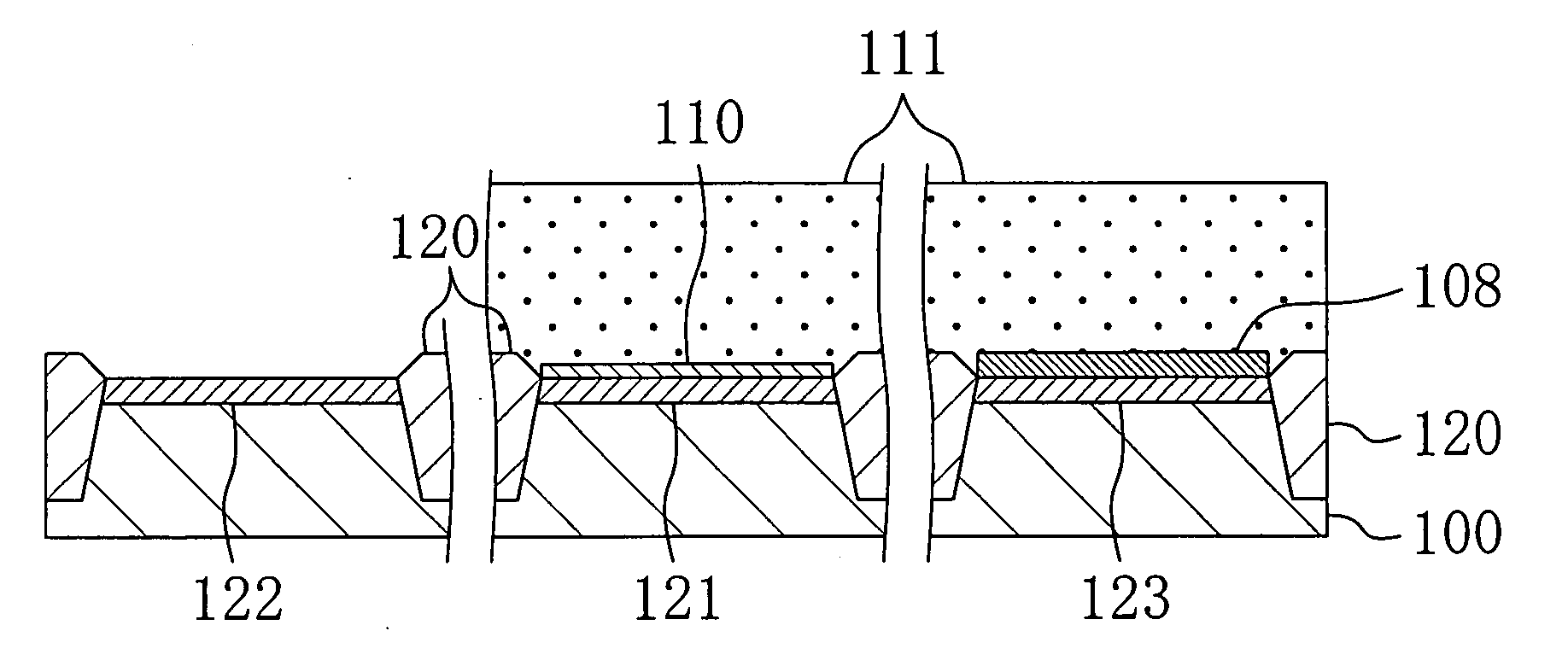
[0023]According to the present invention, the following effects are obtained when compared with the conventional technique. Namely, since the second active region is covered with the protective insulating film when the insulating film to be the first gate insulating film, for example, a silicon oxide film is formed by thermal oxidation, oxidation of the second active region, which is caused due to the thermal oxidation, can be suppressed. This reduces segregation of the impurity implanted in the vicinity of the surface of the substrate in the second active region into the oxide film, so that the impurity concentration in the vicinity of the surface of the substrate in the second active region increases relatively when compared with the case where the insulating film to be the first gate insulating film is formed also on the second active region without covering the second active region with the protective insulating film. As a result, the dose amount in ion implantation for the channel formation to the second active region can be reduced, preventing abnormality of transistor characteristics, such as abnormality of a leakage characteristic at the pn junction.

Problems solved by technology

The above described conventional technique, however, involves abnormality of transistor characteristics in the low leakage MOSFET.

Method used


Image

  • Semiconductor device manufacturing method
  • Semiconductor device manufacturing method
  • Semiconductor device manufacturing method

Examples


embodiment 1

[0038]Description will be given below with reference to the accompanying drawings to a semiconductor device manufacturing method according to Embodiment 1 of the present invention, specifically, a method for manufacturing a MOS semiconductor device including three kinds of gate insulating films of which thicknesses are different from one another.

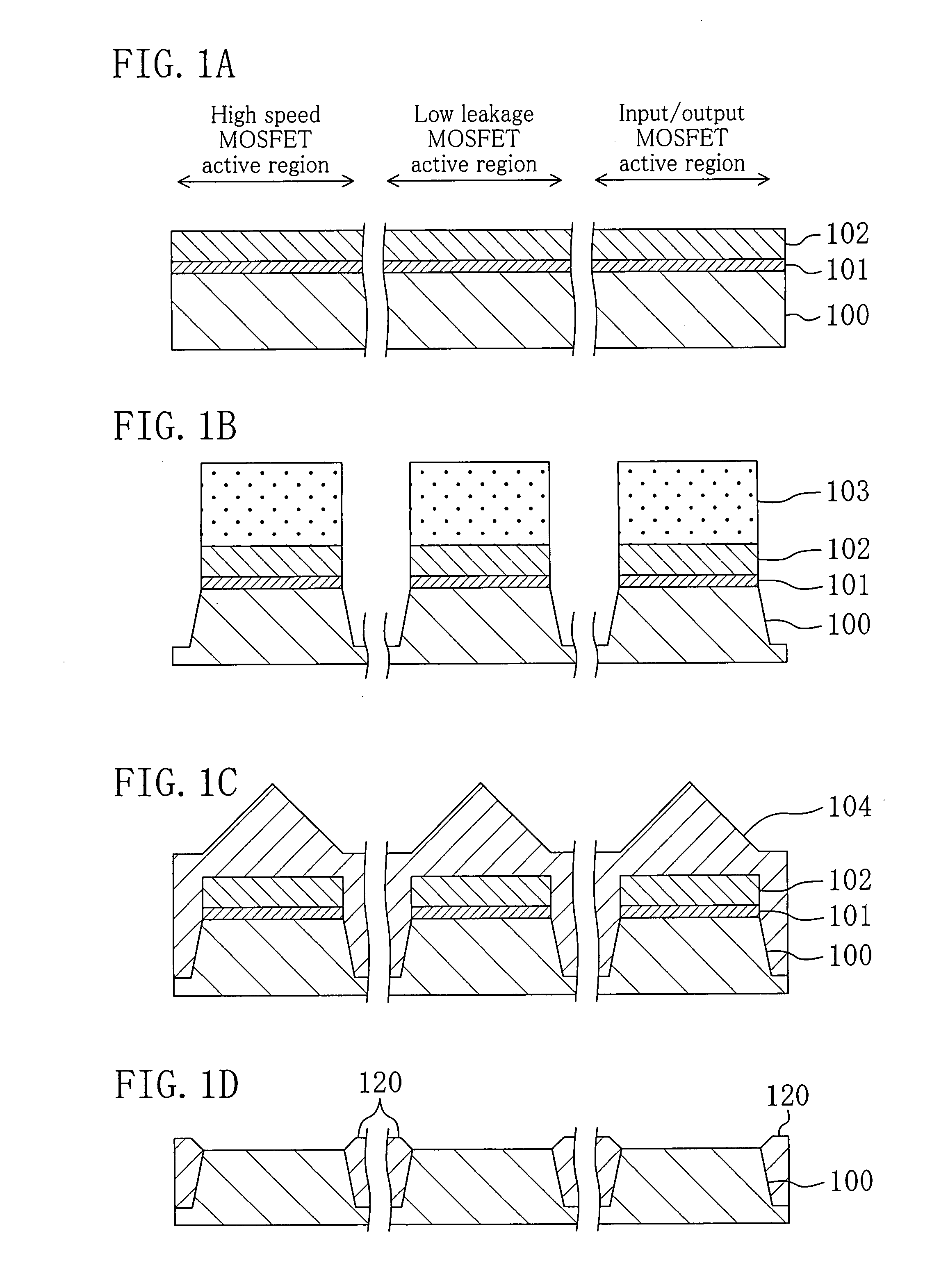
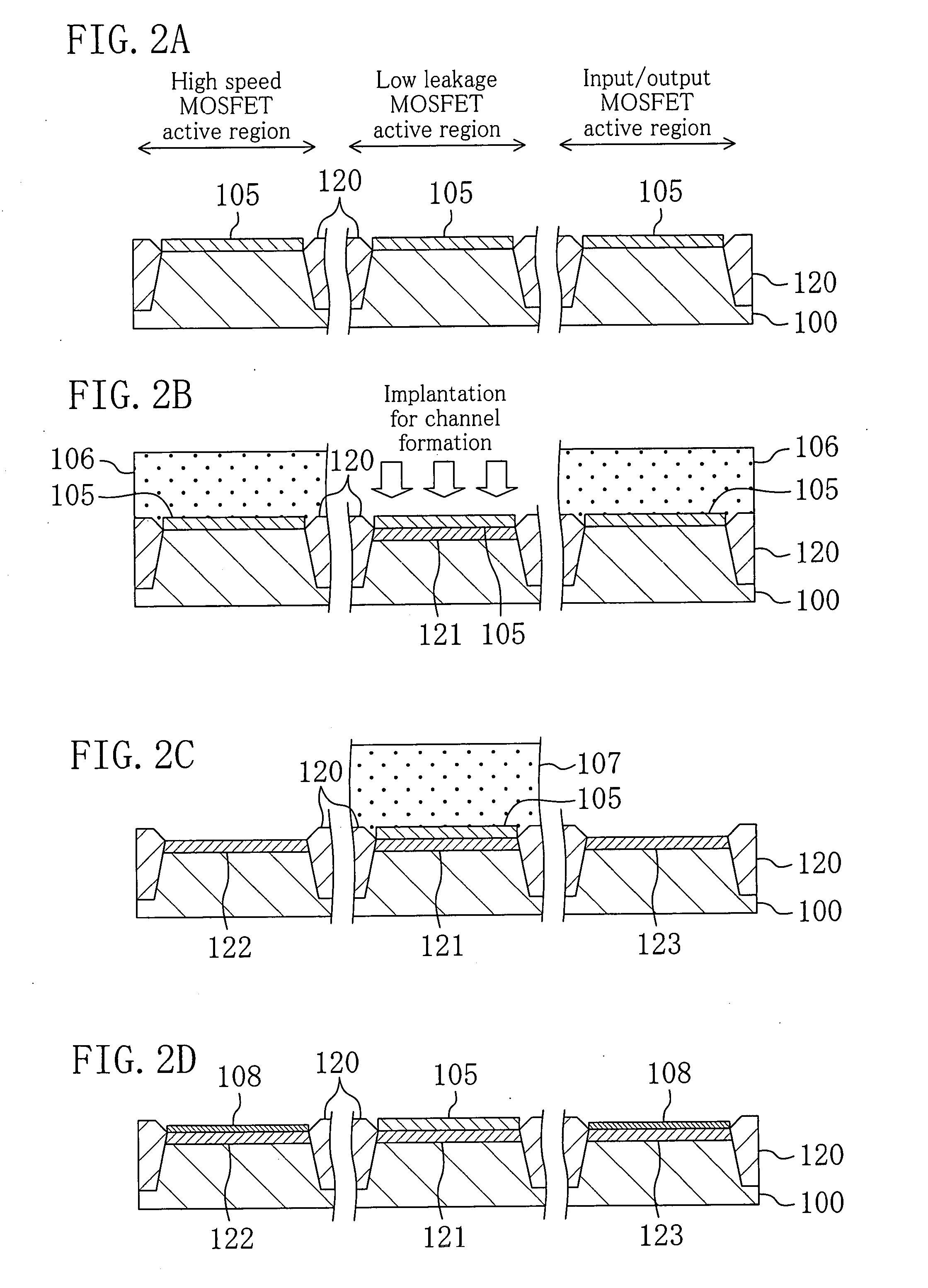
[0039]FIG. 1A to FIG. 1D, FIG. 2A to FIG. 2D, FIG. 3A to FIG. 3C, and FIG. 4A to FIG. 4B are sectional views showing respective steps of the semiconductor device manufacturing method according to Embodiment 1.

[0040]First, as shown in FIG. 1A, a pad oxide film 101 having a thickness of approximately 15 nm and a silicon nitride film 102 having a thickness of approximately 120 nm are formed sequentially on a semiconductor substrate, for example, a silicon substrate 100. Then, as shown in FIG. 1B, the silicon nitride film 102, the pad oxide film 101, and the silicon substrate 100 are subjected to dry etching using a resist pattern 103 open at pa...

embodiment 2

[0054]Description will be given below with reference to the accompanying drawings to a semiconductor device manufacturing method according to Embodiment 2 of the present invention, specifically, a method for manufacturing a MOS semiconductor device including three kinds of gate insulating films of which thicknesses are different from one another.

[0055]Difference of Embodiment 2 from Embodiment 1 lies in that steps shown in FIG. 6A to FIG. 6C are performed in place of the steps shown in FIG. 2B and FIG. 2C in Embodiment 1.

[0056]In detail, similarly to the steps shown in FIG. 1A to FIG. 1D and FIG. 2A in Embodiment 1, the protective insulating films 105 are formed on the input / output MOSFET active region, the low leakage MOSFET active region, and the high speed MOSFET active region first, and the P well regions (not shown) are formed in the respective active regions.

[0057]Subsequently, as shown in FIG. 6A, the low leakage MOSFET active region is subjected to ion implantation for chann...

embodiment 3

[0063]Description will be given below with reference to the accompanying drawings to a semiconductor device manufacturing method according to Embodiment 3 of the present invention, specifically, a method for manufacturing a MOS semiconductor device including three kinds of gate insulating films of which thicknesses are different from one another.

[0064]Difference of Embodiment 3 from Embodiment 1 lies in that the step shown in FIG. 2B in Embodiment 1 (the step of ion implantation to the low leakage MOSFET active region) is performed after the step shown in FIG. 2D (the step of forming the silicon oxide film 108 to be the first gate insulating film). Wherein, steps of the ion implantation to the input / output MOSFET active region and to the high speed MOSFET active region are performed at the timings as those in Embodiment 1.

[0065]FIG. 7A to FIG. 7C are sectional views showing respective steps of the semiconductor device manufacturing method according to Embodiment 3.

[0066]In Embodimen...


PUM


Abstract

After protective insulating films are formed on first to third active regions, the protective insulating films formed on the first and third active regions are removed. Subsequently, an insulating film to be a first gate insulating film is formed on each of the first and third active regions, and then, the protective insulating film formed on the second active region is removed. Next, an insulating film to be a second gate insulating film is formed on the second active region, and then, the insulating film to be the first gate insulating film formed on the third active region is removed. Finally, an insulating film to be a third gate insulating film is formed on the third active region.

Description

FIELD OF THE INVENTION[0001]The present invention relates to a method for manufacturing a MOS semiconductor device including three kinds of gate insulating films of which thicknesses are different from one another.BACKGROUND ART[0002]Conventionally, in MOS (metal-oxide semiconductor) semiconductor device manufacturing methods, there has been employed a process of forming two kinds of gate insulating films having different thicknesses in a single chip. For example, in semiconductor devices in 65 nm design rule generation, a high speed MOSFET (FET: field-effect transistor) including a thin gate insulating film having a thickness of approximately 2.2 nm is provided in an internal circuit operated at 1.2 V while an input / output MOSFET including a thick gate insulating film having a thickness of approximately 7.5 nm is provided in an input / output circuit operated at 3.3 V.[0003]Currently, there are being examined a semiconductor device in which a low leakage MOSFET that lays weight on a ...

Claims


Application Information

Patent Timeline
IPC IPC(8): H01L21/336
CPCH01L21/823412H01L29/7833H01L21/823462
Inventor ARAI, HIDEYUKINAKABAYASHI, TAKASHIOKUNO, YASUTOSHI
Owner GK BRIDGE 1
Learn More