Semiconductor integrated circuit device

a technology of integrated circuit and semiconductor, which is applied in the direction of semiconductor devices, semiconductor/solid-state device details, diodes, etc., can solve the problems of noise interference between the blocks, difficulty in adequately lowering the impedance at the single connection point, and increasing the noise level, so as to suppress noise interference, prevent electrostatic breakdown, and reduce the impedance

Active Publication Date: 2007-12-06
PANASONIC SEMICON SOLUTIONS CO LTD
View PDF2 Cites 2 Cited by
  • Summary
  • Abstract
  • Description
  • Claims
  • Application Information

AI Technical Summary

Benefits of technology

[0008]In view of the above conventional problem, it is an object of the present invention to provide a semiconductor IC device capable of balancing the protection against noise interference with the protection against electrostatic breakdown.
[0009]In order to achieve this object, the present invention provides a semiconductor integrated circuit device which includes a plurality of terminals having a same function. The terminals consist of a plurality of source terminals or ground terminals. The semiconductor integrated circuit device comprises: a plurality of lead frames having the terminals, respectively; a plurality of wire groups each consisting of two or more wires, wherein the wire groups are connected to each other at a single point on the respective lead frames; and a plurality of pad groups each consisting of two or more pads, wherein the pad groups are associated, respectively, with the terminals, and at least one of the pads making up of one of the pad groups is connected to the remaining pad groups, to define an inter-pad connection line. While each of the pad groups is separated from an associated one of the lead frames before a wire bonding process, it is connected to the associated lead frame using one of the wire groups which is connected to the associated lead frame, with relatively low impedance, through the wire bonding process. Although impedance in source and ground lines relative to functional blocks is not changed, the single point connection with the relatively low impedance makes it possible to suppress noise interference. After the wire bonding process, the terminals are connected to each other through an intra-chip wiring layer and the wires to prevent electrostatic breakdown between the terminals.
[0010]In contrast to the conventional device having the problem about lowering an electrostatic breakdown level in conjunction with suppressing noise interference, the semiconductor IC device of the present invention makes it possible to balance the protection against noise interference with the protection against electrostatic breakdown.
[0011]As above, the semiconductor IC device of the present invention can suppress noise interference while protecting against electrostatic breakdown, in a smaller surface area.

Problems solved by technology

Late years, in semiconductor IC devices, a noise level has become increasingly higher due to increase in operating frequency associated with progress in higher processing speed.
In reality, elements, such as the wire 802 and the lead frame 801, in a terminal area between the pad 803 and the outside of a semiconductor package, have a certain level of impedance, and it is difficult to adequately lower the impedance at the single connection point, which is liable to cause the problem of noise interference between the blocks.
However, if the current supplied from the terminal is increased beyond the allowable range, or a plurality of terminals are provided for the purpose of noise reduction, the following problem will occur.

Method used


Image

  • Semiconductor integrated circuit device
  • Semiconductor integrated circuit device
  • Semiconductor integrated circuit device

Examples


first embodiment

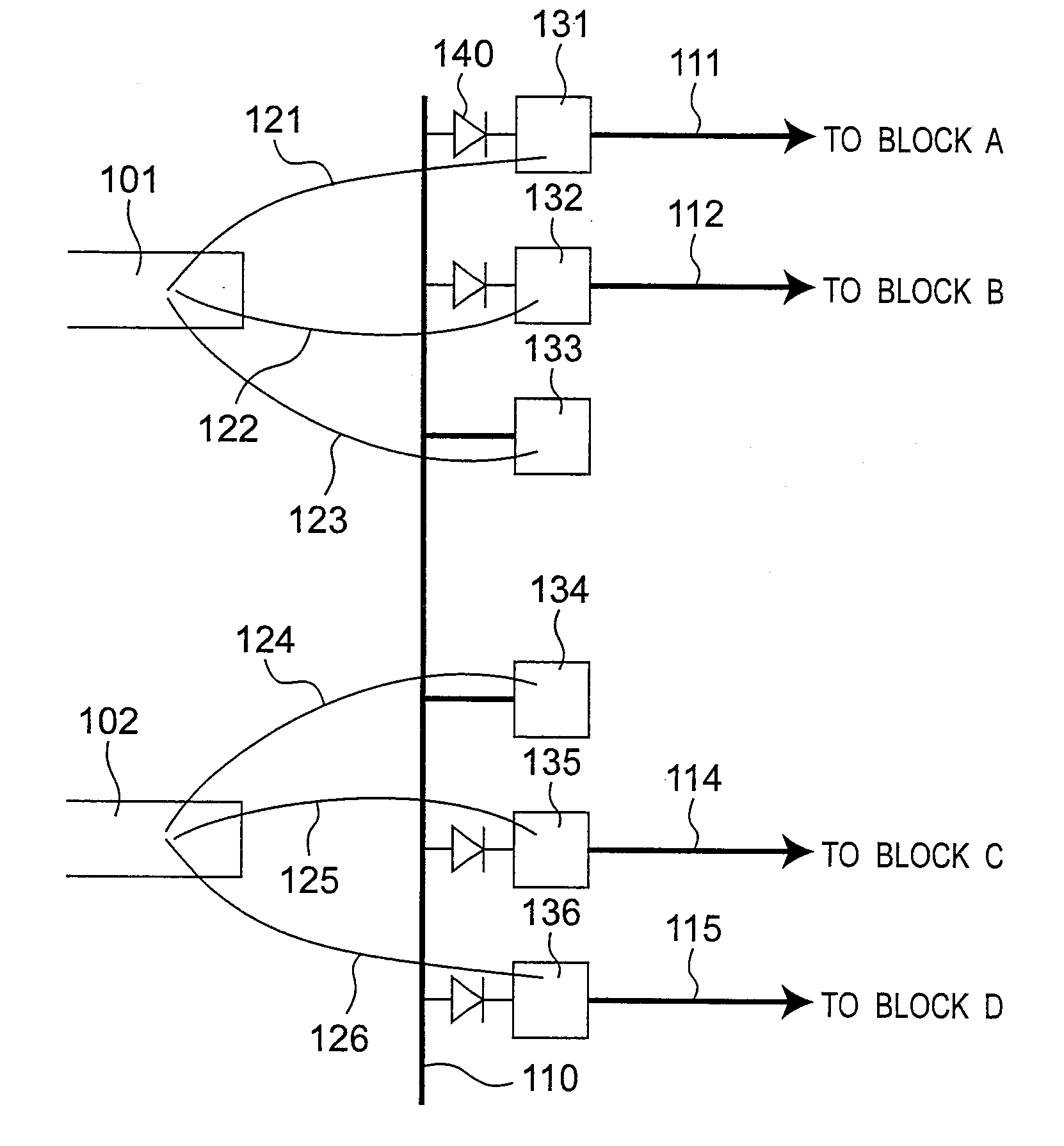
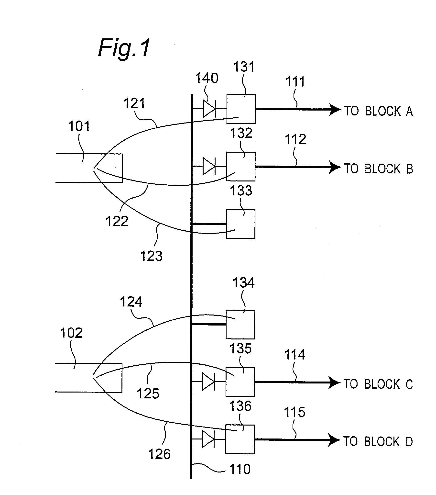
[0023]With reference to FIGS. 1 and 2, a first embodiment of the present invention will be described below. As shown in FIG. 1, a semiconductor IC device according to the first embodiment comprises a first lead frame 101, and two block-dedicated pads 131, 132 which are associated, respectively, with a block A and a block B, and provided for connection between the first lead frame 101 and each of the blocks A, B. The block-dedicated pad 131 is connected to an intra-chip wire 111 connected to the block A, and further connected to a block-dedicated wire 121 for the block A, and an inter-lead-frame connection line 110 for interconnecting between the first lead frame 101 and other lead frame, such as an after-mentioned second lead frame 102. The block-dedicated pad 132 is connected to an intra-chip wire 112 connected to the block B, and further connected to a block-dedicated wire 122 for the block B, and the inter-lead-frame connection line 110. The semiconductor IC device further includ...

second embodiment

[0030]With reference to FIG. 3, a second embodiment of the present invention will be described below. In FIG. 3, the same component or element as that in the first embodiment illustrated in FIG. 1 is defined by the same reference numeral or code, and its detailed description will be omitted. In the semiconductor IC device according to the first embodiment which is designed to connect the block-dedicated and connection wires to each other at a single point on the lead frame (101, 102) by a wire bonding process so as to reduce noise interference, the wire connections and the inter-lead-frame connection line 110 are effective in preventing electrostatic breakdown after the wire bonding process. However, the semiconductor IC device according to the first embodiment cannot prevent electrostatic breakdown during and before the wire bonding process.

[0031]In a semiconductor IC device according to the second embodiment, as shown in FIG. 3, an electrostatic-breakdown protection element 301 is...

third embodiment

[0032]With reference to FIGS. 5 to 7, a third embodiment of the present invention will be described below. In FIGS. 6 and 7, the same component or element as that in the first embodiment illustrated in FIG. 1 is defined by the same reference numeral or code, and its detailed description will be omitted. As compared with the first and second embodiments, a semiconductor IC device according to the third embodiment is deigned to more efficiently protect against electrostatic breakdown in more small surface area.

[0033]Specifically, as shown in FIG. 5, in the semiconductor IC device according to the third embodiment, a semiconductor substrate having a first conductivity type has a first well having a second conductivity type which is opposite to the first conductivity type, and a second well having the first conductivity type exists in the first well. Further, an electrostatic-breakdown protection element is connected between a source line and a ground line. The ground line is divided in...


PUM


Abstract

Disclosed is a semiconductor IC device capable of suppressing the interference of noise generated in one functional block with other functional blocks therein while protecting against electrostatic breakdown. A plurality of isolated pads are connected to a first terminal through respective wires, and further connected to a plurality of isolated pads each connected to a second terminal having the same function as that of the first terminal, so as to reduce noise interference based on the pad isolation and protect against electrostatic breakdown based on the inter-pad connection.

Description

RELATED APPLICATION[0001]This application is based on Japanese Patent Application No. 2006-151439, the contents of which are incorporated herein by reference.BACKGROUND OF THE INVENTION[0002]The present invention relates to a technique for reducing the influence of noise generated in a functional block on other functional blocks in a semiconductor integrated circuit (IC) device, and more particularly to a semiconductor IC device adapted to balance the protection against noise interference with the protection against electrostatic breakdown, i.e., surge.[0003]Late years, in semiconductor IC devices, a noise level has become increasingly higher due to increase in operating frequency associated with progress in higher processing speed. Under such a situation, there has been proposed a technique of reducing noise interference between a plurality of functional blocks (each hereinafter referred to simply as “block”) based on isolation of a pad. FIG. 8 shows one example of this type of tec...

Claims


Application Information

Patent Timeline
Patent Type & Authority Applications(United States)
IPC IPC(8): H01L23/48
CPCH01L23/552H01L2224/0603H01L24/06H01L24/49H01L27/0255H01L2224/48091H01L2224/48245H01L2224/49113H01L2924/01003H01L2924/01004H01L2924/01005H01L2924/01015H01L2924/01074H01L2924/01082H01L2924/14H01L2924/30105H01L2924/30107H01L2924/3011H01L23/60H01L2224/05554H01L24/48H01L2924/01006H01L2924/01033H01L2224/48247H01L2224/05553H01L2924/00014H01L2224/023H01L2224/45099H01L2224/05599H01L2924/0001
Inventor TANAKA, AKIRA
Owner PANASONIC SEMICON SOLUTIONS CO LTD
Why Eureka
Try Eureka