

Method of and apparatus for semiconductor device
a fabrication apparatus and semiconductor technology, applied in the direction of grinding machine components, manufacturing tools, lapping machines, etc., can solve the problems of non-uniform pressure against the polishing pad, difficult to achieve uniform amount of polishing in the area around the edges of semiconductor wafers, etc., to achieve uniform polishing of the surface
- Summary
- Abstract
- Description
- Claims
- Application Information
AI Technical Summary
Benefits of technology
Problems solved by technology
Method used
Image

Examples
first embodiment
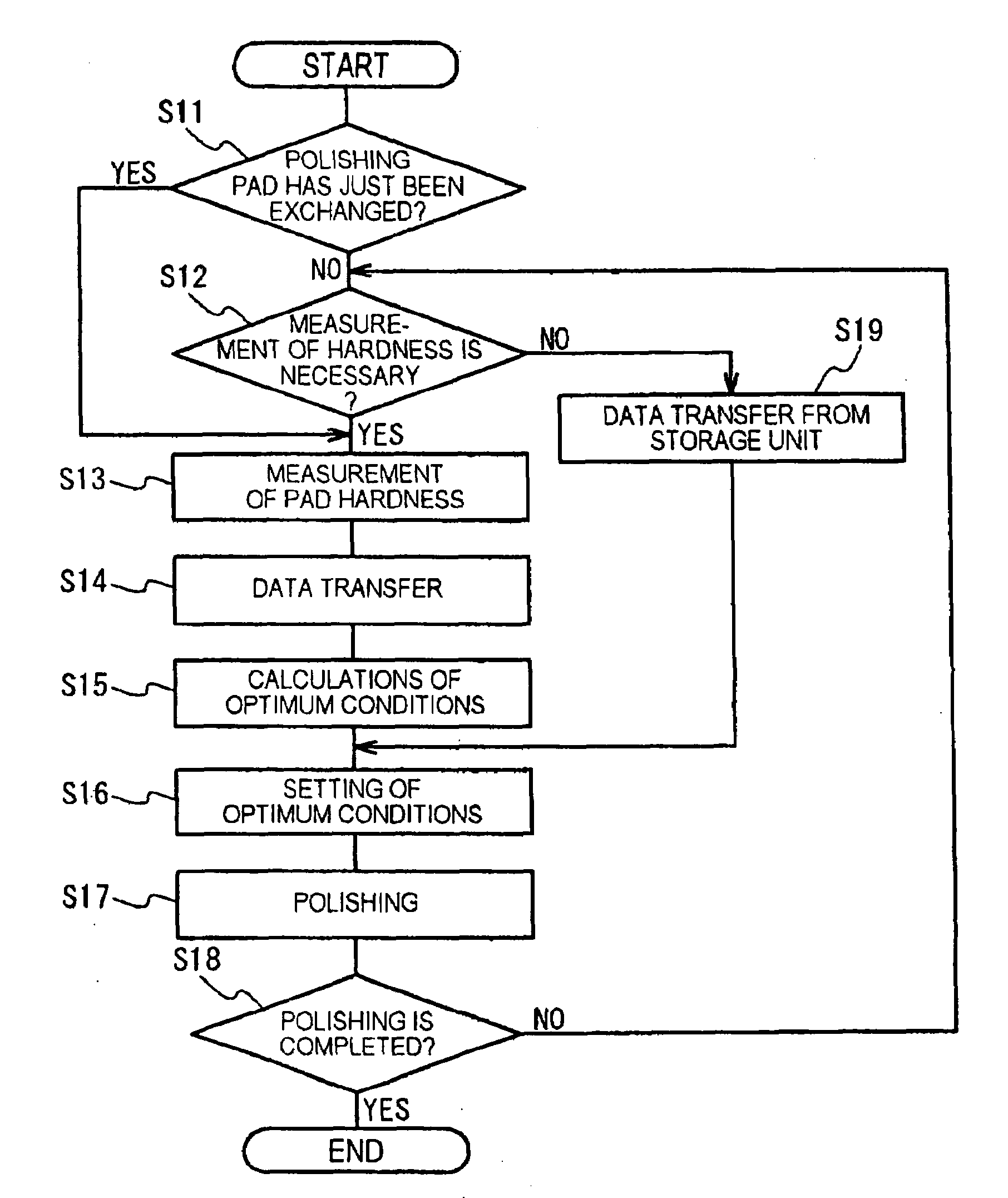
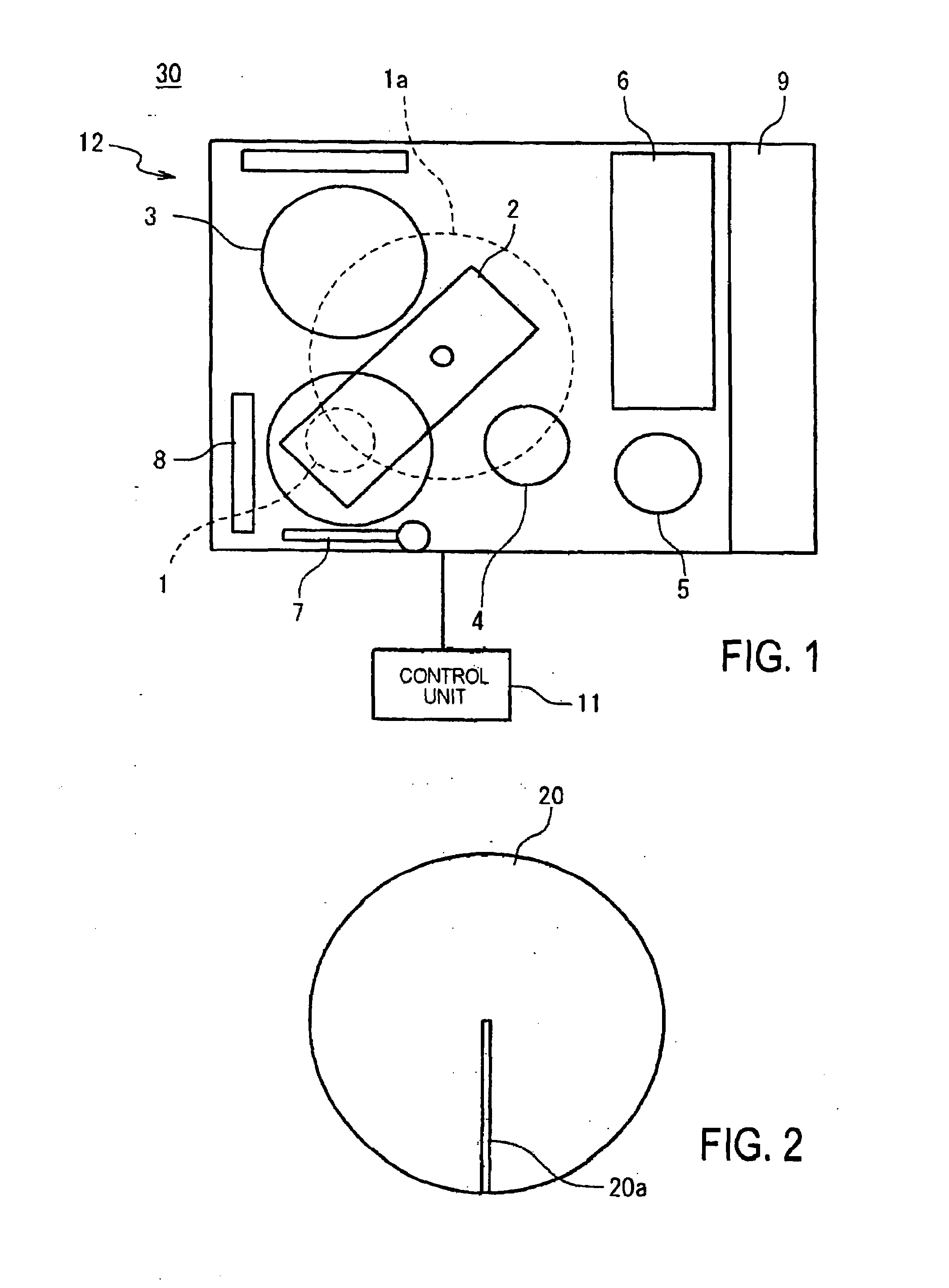
[0039]Semiconductor device fabrication device 30 of the first embodiment shown in FIG. 1 is equipped with: polishing unit 12 for carrying out polishing of a semiconductor wafer; hardness meter 7 for measuring the hardness of a polishing pad; and control unit 11 for controlling the operation of polishing unit 12 and hardness meter 7.
[0040]Polishing unit 12 includes: head 1, cross 2, platen 3, load / unload unit 4, robot 5, cleaning unit 6, dresser 8, and interface 9. The role of each component is described below.
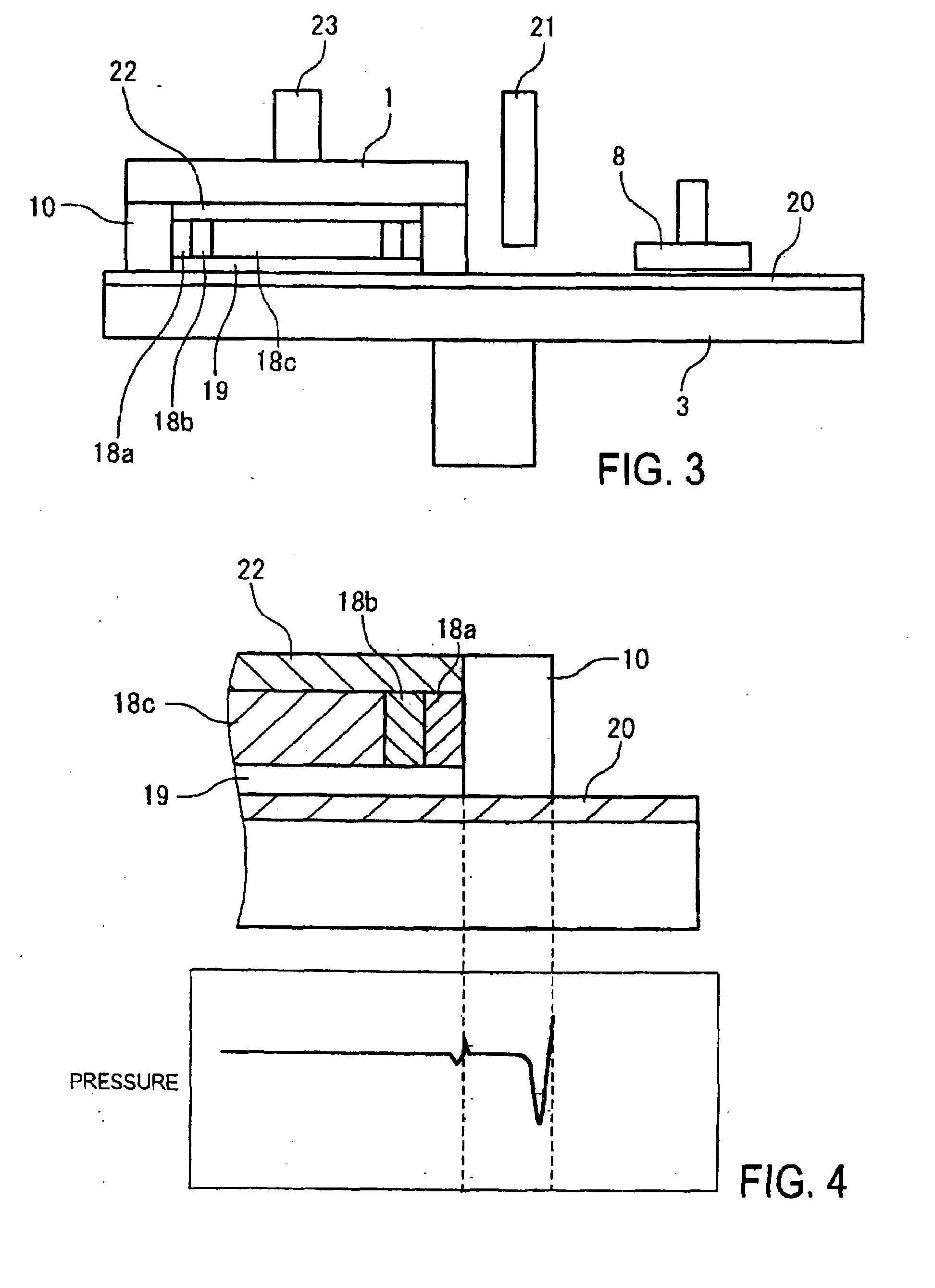
[0041]Head 1 is for holding semiconductor wafer 19. Cross 2 is for supporting head 1, and applies a rotational motion to head 1 that describes head orbit 1a. Platen 3 is a part for affixing polishing pad 20. When polishing semiconductor wafer 19, platen 3 rotates, and polishing is carried out by pressing semiconductor wafer 19 supported on head 1 against polishing pad 20 which is affixed to platen 3. Load / unload unit 4 is a component for attaching and detaching semiconductor wa...
second embodiment
[0072]Explanation next regards the second embodiment. In the second embodiment, the method of calculating the optimum polishing conditions differs from that of the first embodiment. In other words, the functional configuration of control unit 11 is different.
[0073]In contrast to the first embodiment in which the hardness of polishing pad 20 is actually measured and the optimum polishing conditions then found based on the measurement results, in the second embodiment, the hardness of the polishing pad is estimated based on the time interval over which polishing pad 20 is exposed to exhausting conditions and the optimum polishing conditions then found based on this estimated hardness. No hardness meter is therefore necessary in the second embodiment. The configuration of polishing unit 12 is identical to that of the first embodiment, and redundant explanation is therefore omitted. The following explanation regards the functional configuration of control unit 11.
[0074]Control unit 11 i...
third embodiment
[0092]Explanation next regards the third embodiment. The third embodiment provides an additional modification of the functional configuration of control unit 11 compared to the second embodiment. In the second embodiment, the optimum polishing conditions were found from the accumulation of time over which polishing pad 20 is used in the polishing process, but in the third embodiment the optimum polishing conditions are found based on the time interval over which polishing pad 20 is placed in wet idle in addition to the accumulated time of the polishing process. Regarding points other than the functional configuration of control unit 11, the third embodiment is identical to the second embodiment and redundant explanation of these points is therefore omitted.
[0093]As in the second embodiment, control unit 11 includes storage unit 13 and calculation unit 14. Calculation unit 14 realizes the functions of referring to storage unit 13 to find the optimum polishing conditions (P) and takin...
PUM
| Property | Measurement | Unit |
|---|---|---|
| Angle | aaaaa | aaaaa |
| Digital information | aaaaa | aaaaa |
| Digital information | aaaaa | aaaaa |
Abstract
Description
Claims
Application Information