Method of production of multilayer circuit board with built-in semiconductor chip

a multi-layer circuit board and semiconductor chip technology, applied in the direction of semiconductor/solid-state device details, printed circuit non-printed electric components association, conductive pattern formation, etc., can solve the problem of insulating film ending up being peeled off from the semiconductor chip, and the back surface of smoothly polished will have insufficient bondability with the insulating film laid, so as to achieve the effect of strengthening the bondability

Active Publication Date: 2006-11-14
SHINKO ELECTRIC IND CO LTD
View PDF10 Cites 19 Cited by
  • Summary
  • Abstract
  • Description
  • Claims
  • Application Information

AI Technical Summary

Benefits of technology

[0006]An object of the present invention is to provide a method of production of a multilayer circuit board incorporating a semiconductor chip whi

Problems solved by technology

Such a semiconductor chip polished on its back surface, however, creates the following problem in the process of production of a multilayer circuit board.
That is, when placing the semiconductor chip to be built in, with its active surface facing down, on a lower interconnect layer and then forming an insulating film over it, sometimes the smoothly polished back surface will have insuf

Method used


Image

  • Method of production of multilayer circuit board with built-in semiconductor chip
  • Method of production of multilayer circuit board with built-in semiconductor chip
  • Method of production of multilayer circuit board with built-in semiconductor chip

Examples


first embodiment

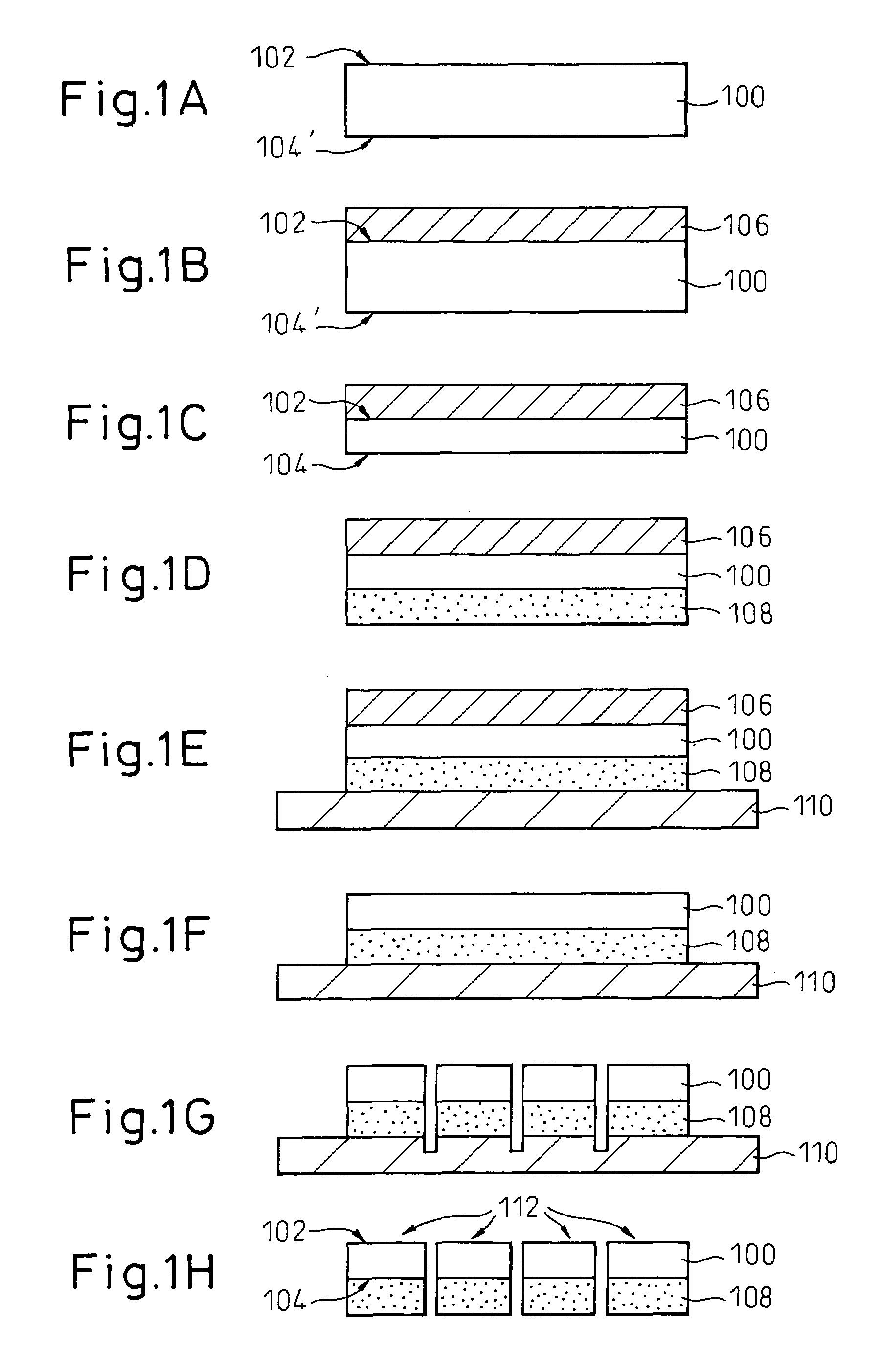
[0021]Referring to FIGS. 1A to 1H, an explanation will be made of an example of coating a coupling agent on the back surface of a semiconductor chip according to a first embodiment of the present invention.

[0022]A silicon wafer 100 shown in FIG. 1A is formed with a large number of semiconductor chips at its semiconductor chip forming surface 102. The wafer 100 is for example a thickness of 725 μm or so.

[0023]As shown in FIG. 1B, a surface protective tape 106 is adhered to the semiconductor chip formation surface 102. This is performed using a laminator at ordinary temperature by rolling.

[0024]As shown in FIG. 1C, the back surface 104′ of the silicon wafer 100 is polished to obtain the polished back surface 104. This polishing is performed using a back grinder at 4000 rpm at 1 μm / sec. The thickness of the wafer 100 is reduced to about 20 to 100 μm or so.

[0025]As shown in FIG. 1D, the characterizing feature of the first embodiment of the present invention is the formation of the layer...

second embodiment

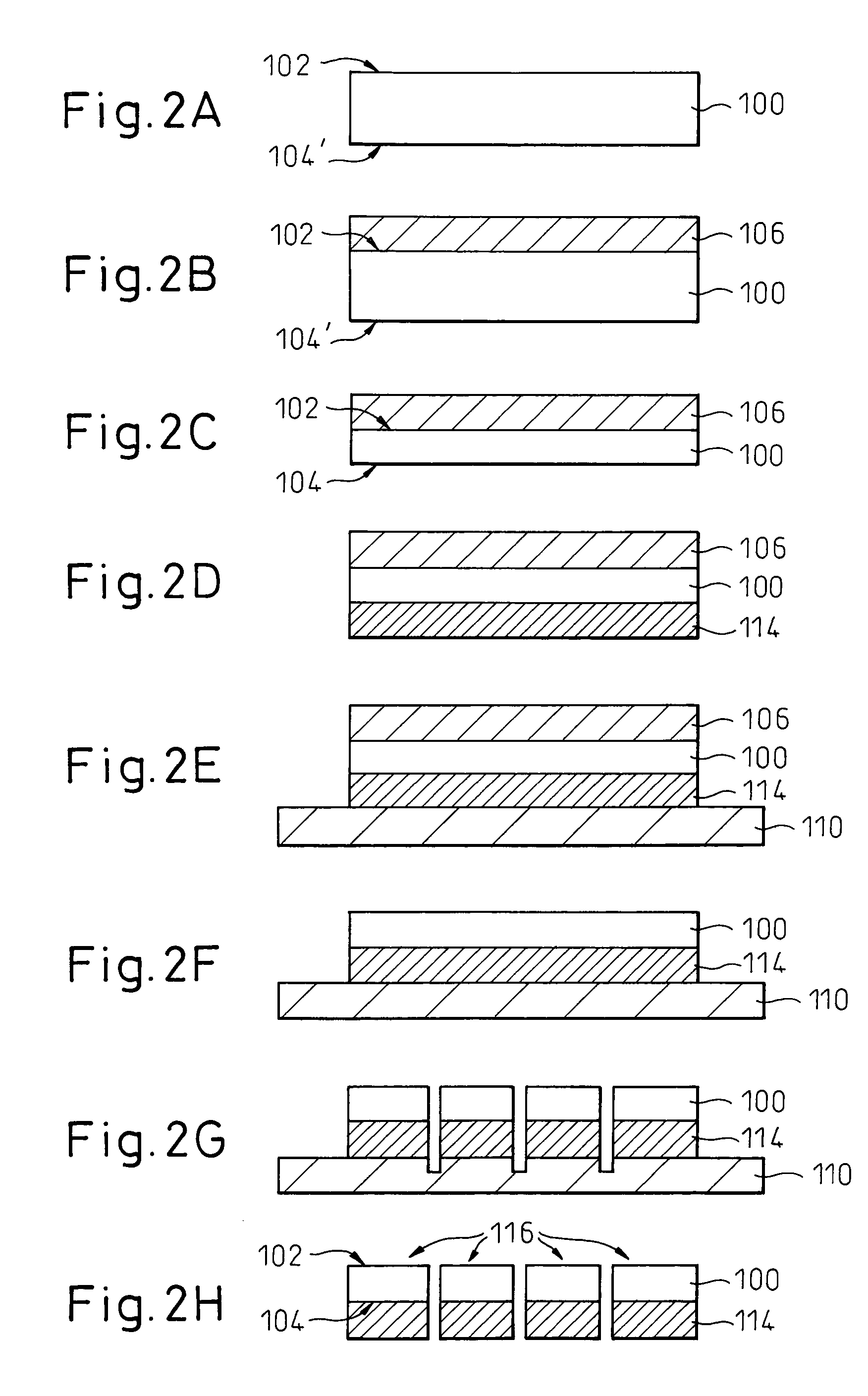
[0033]Next, an explanation will be made of an example of bonding a bonding film on the back surface of a semiconductor chip according to a second embodiment of the present invention.

[0034]In the same way as the steps of FIG. 1A to FIG. 1C of the first embodiment, the steps of FIG. 2A to FIG. 2C are performed to polish the back surface 104′ of the silicon wafer 100 to the polished back surface 104.

[0035]Next, as shown in FIG. 2D, the second embodiment of the present invention is characterized by bonding a bonding film 114 on the polished back surface 104. This is performed for example by using a laminator to bond a die attach film (thickness 25 μm) comprised of an epoxy-based curing resin under conditions of a heating temperature of 140° C., a heating time of 10 sec, and a pressing force of 1 MPa.

[0036]After this, in the same way as the steps of FIG. 1E to FIG. 1H of the first embodiment, the steps of FIG. 2E to FIG. 2H are performed. Each diced semiconductor chip 116 has an active s...

third embodiment

[0038]Next, an explanation will be made of an example of roughening a polished back surface of a silicon chip according to a third embodiment of the present invention.

[0039]In the same way as the steps of FIG. 1A to FIG. 1C of the first embodiment, the steps of FIG. 3A to FIG. 3C are performed to polish the back surface 104′ of the silicon wafer 100 to the polished back surface 104.

[0040]Next, as shown in FIG. 3D, the third embodiment of the present invention is characterized by roughening the polished back surface 104 to obtain the roughened back surface 104R. This is performed for example by using a plasma etcher for isotropic dry etching by an SF6 / Ar mixed gas under conditions of a gas pressure of 100 Pa to give a roughness of 0.1 μm.

[0041]After this, in the same way as the steps of FIG. 1E to FIG. 1H of the first embodiment, the steps of FIG. 3E to FIG. 3H are performed. Each diced semiconductor chip 118 has an active surface 102 and a back surface 104R. The back surface 104R is...


PUM


Abstract

A method of production of a multilayer circuit board comprised of a multilayer structure circuit formed by a plurality of interconnect layers and insulation layers stacked together and a semiconductor chip included therein, including the steps of placing a semiconductor chip having a polished back surface, with its active surface facing downward, on an already formed lower interconnect layer and forming an insulation layer over the layer on which the semiconductor chip has been placed, the method further including the step of treating the polished back surface of the semiconductor chip to improve its bondability with the insulation layer before the step for formation of the insulation layer.

Description

BACKGROUND OF THE INVENTION[0001]1. Field of the Invention[0002]The present invention relates to a method of production of a multilayer circuit board comprised of a multilayer structure circuit formed by a plurality of interconnect layers and insulation layers stacked together and a semiconductor chip included therein.[0003]2. Description of the Related Art[0004]Multilayer circuit boards with built-in semiconductor chips are being widely used as thin boards. The built-in semiconductor chips have to be made as thin as possible in order for them to fit in the limited board thickness. As means for this, the practice has been to polish the back surfaces so as to reduce the thickness of the semiconductor chips (for example, see US 2001 / 0008794A1, [00103] to [0110]). Such a semiconductor chip polished on its back surface, however, creates the following problem in the process of production of a multilayer circuit board.[0005]That is, when placing the semiconductor chip to be built in, with...

Claims


Application Information

Patent Timeline
IPC IPC(8): H05K3/30H05K3/02H05K3/10H01L23/12H01L21/68H01L21/78H01L23/24H01L23/538H05K1/18H05K3/46
CPCH01L21/6835H01L23/24H01L23/5389H01L24/27H01L24/29H01L21/6836Y10T29/49155H01L21/78H01L2221/68327H01L2221/6834H01L2221/68363H01L2224/04026H01L2224/16225H01L2224/274H01L2224/73253H01L2224/83191H01L2924/01004H01L2924/01013H01L2924/01018H01L2924/01029H01L2924/01033H01L2924/01074H01L2924/01078H01L2924/01079H01L2924/10158H01L2924/15153H01L2924/1517H01L2924/16195H05K1/185H05K3/4644H01L2924/01006H01L2924/01019H01L2924/01072H01L2924/10253Y10T29/4913H01L2224/0401Y10T29/49146H01L2924/00H01L2924/12042A63G9/00
Inventor SUNOHARA, MASAHIROMURAYAMA, KEIHIGASHI, MITSUTOSHI
Owner SHINKO ELECTRIC IND CO LTD
Why Eureka
Try Eureka