Signal processing circuit

a technology of signal processing and circuit, applied in the direction of transmission, information storage, instruments, etc., can solve the problem of difficult to ensure this certain

Inactive Publication Date: 2007-12-06
QIMONDA
View PDF3 Cites 39 Cited by
  • Summary
  • Abstract
  • Description
  • Claims
  • Application Information

AI Technical Summary

Benefits of technology

[0022]An advantage of the embodiments of the present invention is that the first clock signal and the second clock signal can more easily be aligned with respect to each other. As a consequence, the data transfer rate can more easily be increased without risking the negative influence on exchanging data between the first circuit and the second circuit. Furthermore, due to the alignment of the first clock signal and the second clock signal, the overall circuitry of the signal processing circuit can be simplified, as complex synchronization circuits can be omitted, which usually require an elaborate training scheme.

Problems solved by technology

As both clock signals are created at different sites inside a controller circuit, for instance, a graphics processing unit (GPU) and as both clock signals are distributed via different paths or clock signal lines on their way to the DRAM memory circuits, it is difficult to ensure this certain alignment of the data clock signal RDQS and the clock signal CK with respect to each other.

Method used


Image

  • Signal processing circuit
  • Signal processing circuit
  • Signal processing circuit

Examples


second embodiment

[0032]Before describing the present invention in more detail, it should be noted that objects with the same or similar functional properties are denoted with the same reference signs. Unless explicitly noted otherwise, the description with respect to objects with similar or equal functional properties can be exchanged with respect to each other.

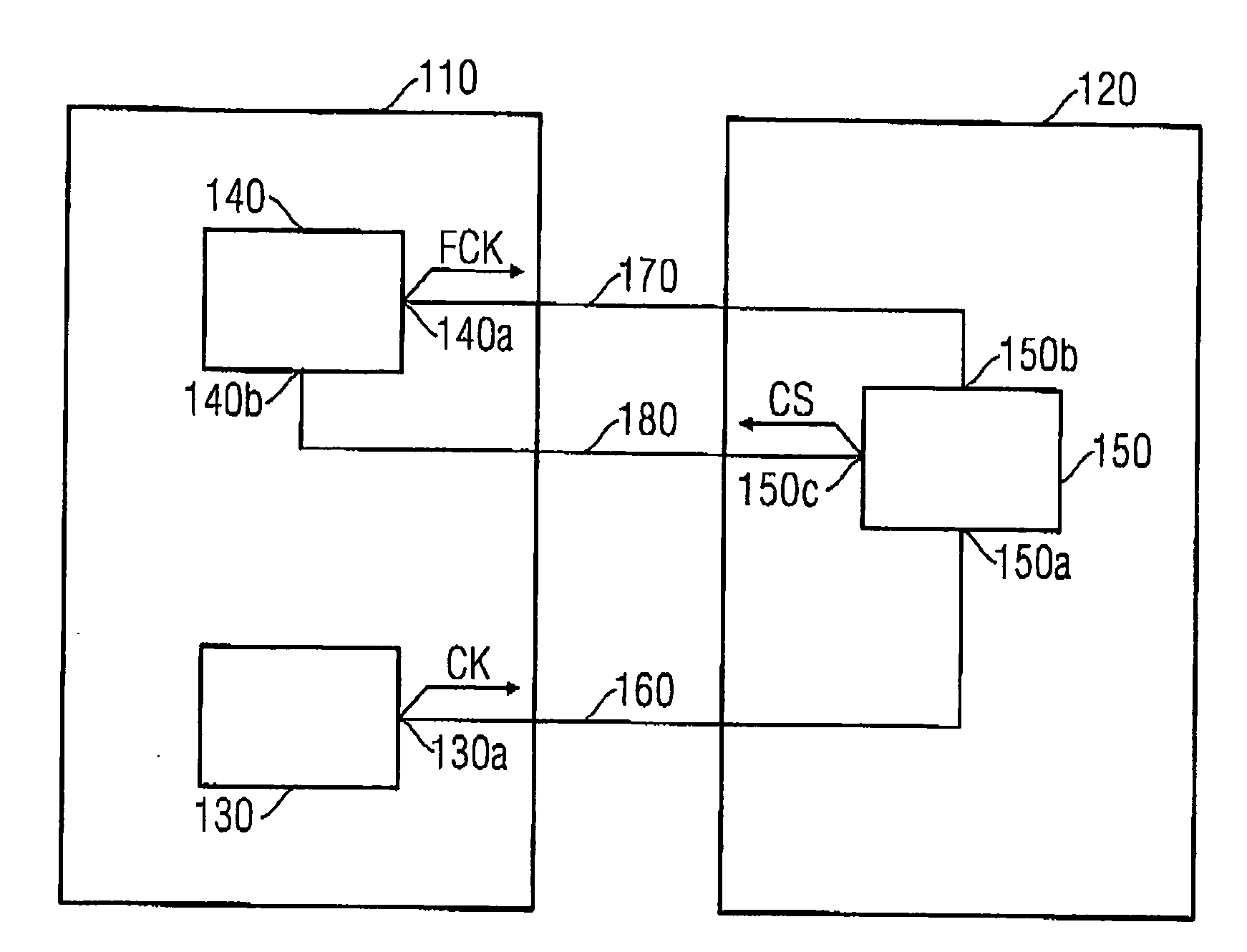
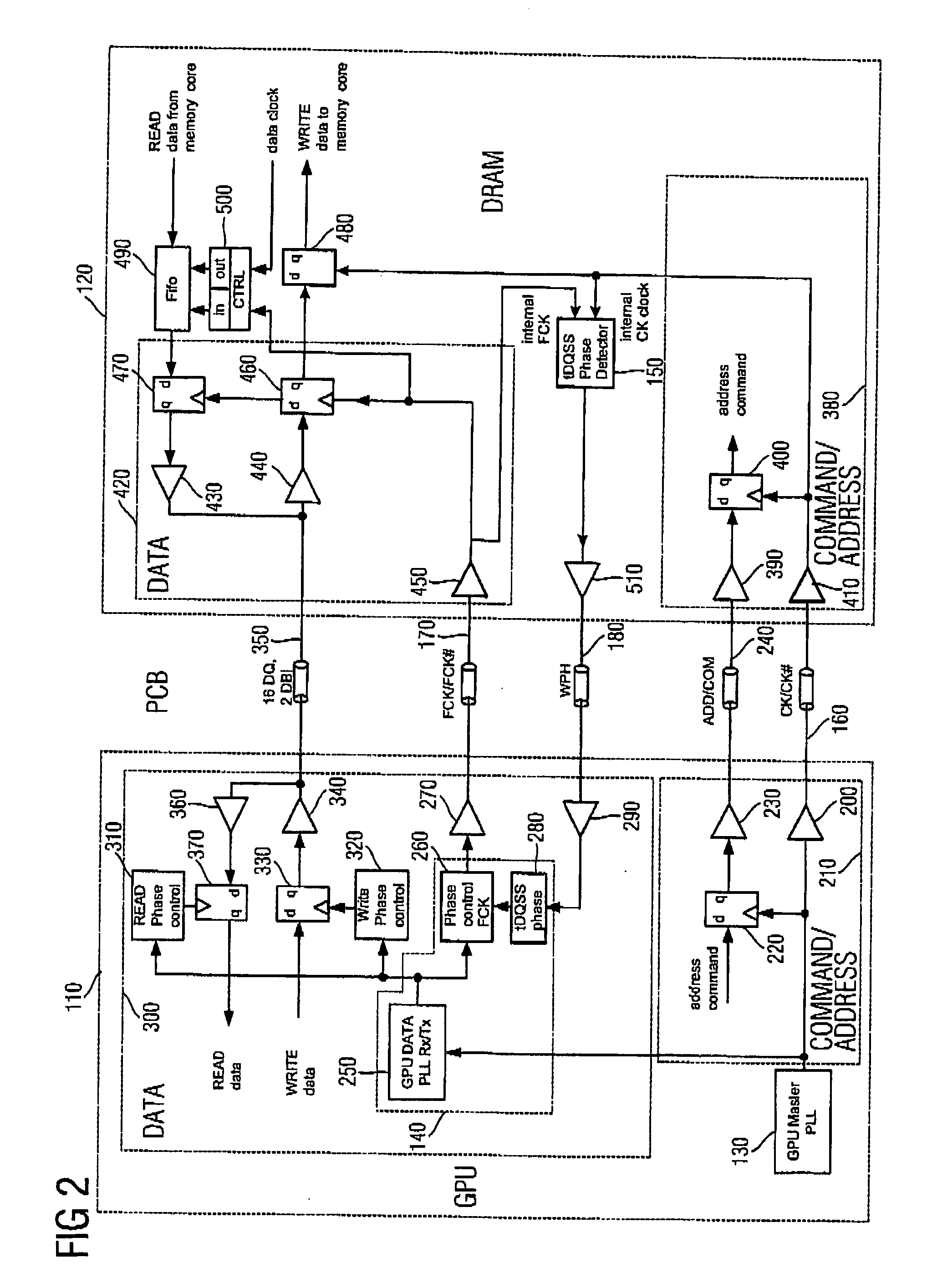
[0033]FIG. 2 shows a second embodiment of an inventive signal processing circuit 100. The signal processing circuit 100 comprises a first circuit 110, which is in the embodiment shown a graphical processing unit (GPU). Furthermore, the signal processing circuit 100 also comprises a second circuit 120, which is here a DRAM memory circuit. The GPU 110 and the DRAM memory 120 are mounted on a printed circuit board (PCB), as shown in FIG. 2.

[0034]The inventive signal processing circuit 100 shown in FIG. 2 also comprises a first clock signal generator 130, which is the GPU master PLL circuit (PLL=Phase Lock-Loop) providing a first clock signal CK ...

third embodiment

[0045]While FIG. 2 shows a schematic, more basic representation of an inventive signal processing circuit 100, FIG. 3 shows a more concrete implementation as an inventive signal processing circuit 100 in the framework of a high speed memory controller circuit and memory circuit in the field of computer graphics. With respect to the embodiments shown in FIG. 3, a FCK / CK training loop will also be discussed in more detail later. FIG. 3 shows an embodiment of an inventive signal processing circuit, which differs only slightly from the embodiment shown in FIG. 2. To be more precise, the embodiment shown in FIG. 3 comprises an additional WPH frame generator 600 (WPH=write phase), which is connected to the output of the phase detector 150. Furthermore, the WPH frame generator 600 is connected to the output of the latch 460 receiving write phase data from the output q of the latch 460. An output of the WPH frame generator 600 is connected to an input d of a latch 610. An output q of the la...


PUM


Abstract

A signal processing circuit includes a first circuit including a first clock signal generator with an output for a first clock signal and a second clock signal generator with an output for a second clock signal and an input for a comparison signal. The second clock signal is generated by the second clock signal generator based on the comparison signal. A second circuit includes a phase detector with a first input for the first clock signal, with a second input for the second clock signal and an output for the comparison signal indicating a relation between the phases of the first clock signal received at the first input and the second clock signal received at the second input.

Description

TECHNICAL FIELD[0001]The present invention relates to a signal processing circuit, especially a circuit comprising a memory controller or a processor and a memory circuit, for instance, a high-speed memory and a graphics processing unit (GPU).BACKGROUND[0002]In modern high-speed memory circuits, especially in high-speed DRAM circuits (DRAM=Dynamic Random Access Memory), a memory circuit and a memory control circuit or a processor are connected by a unidirectional address / command bus and by a bi-directional data bus. Usually, each of both busses comprises a separate clock line. Sometimes, the data bus comprises a clock strobe line instead of a separate clock line.[0003]In a DRAM memory circuit, the address / command bus usually controls the actions carried out inside the data path of the DRAM memory circuit. All information concerning the timing with respect to commands and address (command / address-timings) is derived from the clock signal of the address / command bus, which is usually r...

Claims


Application Information

Patent Timeline
Patent Type & Authority Applications(United States)
IPC IPC(8): G06F17/50
CPCG11C7/22H04L7/0331H04L7/02G11C7/222G06F1/06G06F1/04
Inventor HEIN, THOMASKHO, REX
Owner QIMONDA
Why Eureka
Try Eureka