Array substrate for liquid crystal display and method of testing

a liquid crystal display and array substrate technology, applied in the direction of semiconductor devices, semiconductor/solid-state device details, instruments, etc., can solve the problems of lowering the productivity of the liquid crystal display production process, and achieve the effect of reducing the process tim

Inactive Publication Date: 2007-12-13
SAMSUNG ELECTRONICS CO LTD
View PDF0 Cites 39 Cited by
  • Summary
  • Abstract
  • Description
  • Claims
  • Application Information

AI Technical Summary

Benefits of technology

[0020] According to the above, the fuse is opened when the current higher than the reference current is applied thereto. Thus, a laser trimming process, which is performed to insulate the signal line from the test line, can be omitted, so that the process time can be shortened.

Problems solved by technology

A laser trimming process is performed to cut the test lines after the fault inspection process for the signal lines and the pixels has been finished that may result in an overload, thereby lowering the productivity of the liquid crystal display production process.

Method used


Image

  • Array substrate for liquid crystal display and method of testing
  • Array substrate for liquid crystal display and method of testing
  • Array substrate for liquid crystal display and method of testing

Examples


Embodiment Construction

[0036] Hereinafter, the present invention will be explained in detail with reference to the accompanying the drawings.

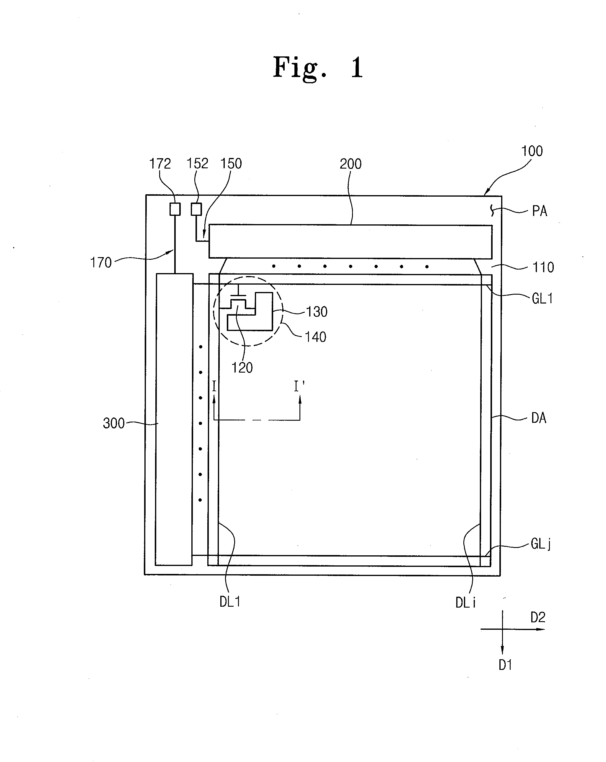
[0037]FIG. 1 is a plan view illustrating an array substrate according to an exemplary embodiment of the present invention.

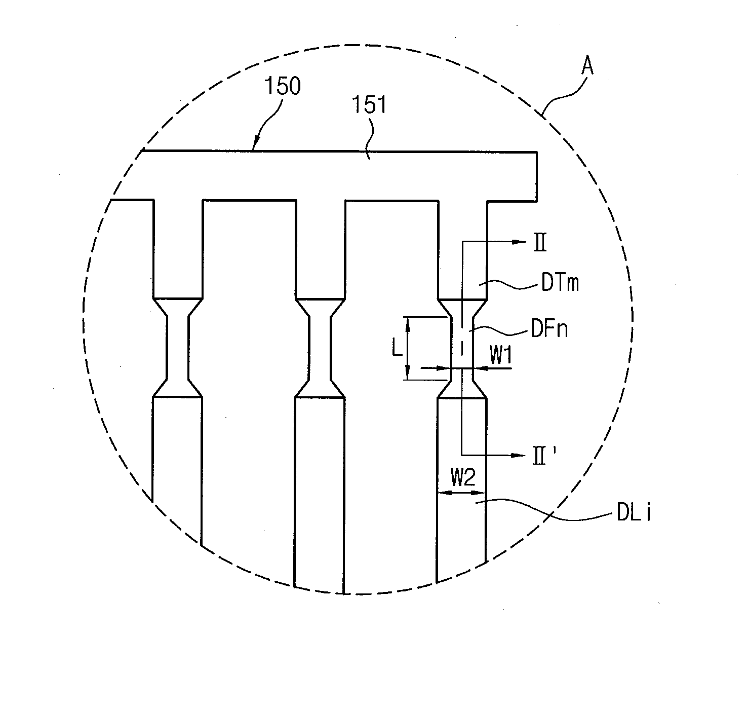
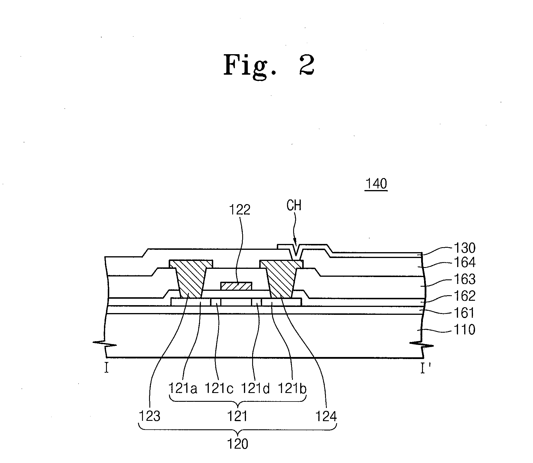
[0038] Referring to FIG. 1, the array substrate 100 includes a first base substrate 110, a plurality of data lines DL1, . . . , and DLi, a plurality of gate lines GL1, . . . , and GLj, and a plurality of the pixels 140 and a data test line 150.

[0039] The first base substrate 110 includes a material that allows light to pass therethrough, for instance glass, quartz, sapphire or silicon. The first base substrate 110 is divided into a display area DA, in which the image is displayed, and a peripheral area PA, which surrounds the display area DA. The image is not displayed in the peripheral area PA.

[0040] The data lines DL1, . . . , and DLi are formed on the first base substrate 110 while extending in the first direction D1. The data lines DL1, . ...


PUM


Abstract

An array substrate including a signal line, a test line to inspect the open of the signal line and fault of the pixels, and a fuse electrically connecting the signal line with the test line. The fuse is opened when a current higher than a reference current is applied thereto. Accordingly, a laser trimming process to insulate the signal line from the test line is not needed after the signal line and pixels have been tested, so that the processing time may be shortened.

Description

CROSS-REFERENCE TO RELATED APPLICATION [0001] This application relies for priority upon Korean Patent Application No. 2006-45796 filed on May 22, 2006, the contents of which are herein incorporated by reference in its entirety. BACKGROUND OF THE INVENTION [0002] 1. Field of the Invention [0003] The present invention relates to improving the production of liquid crystal displays and, more particularly, to improving the production of array substrates and a method of testing the same. [0004] 2. Description of the Related Art [0005] A liquid crystal display includes an array substrate formed with pixels, a color filter substrate facing the array substrate, and a liquid crystal layer interposed between the array substrate and the color filter substrate. [0006] The pixels are aligned on the array substrate in an array form to provide the liquid crystal layer with pixel voltages. The array substrate includes signal lines which transmit image signals to the pixels. For instance, the array s...

Claims


Application Information

Patent Timeline
Patent Type & Authority Applications(United States)
IPC IPC(8): H01L23/58
CPCG02F1/1362H01L23/5256G02F2001/136254G02F1/136254H01L2924/0002H01L2924/00G02F1/1345
Inventor YOON, JI-HWAN
Owner SAMSUNG ELECTRONICS CO LTD
Why Eureka
Try Eureka