High-efficiency, overvoltage-protected, light-emitting semiconductor device

a semiconductor device, high-efficiency technology, applied in the direction of semiconductor devices, basic electric elements, electrical appliances, etc., can solve the problem of insufficient resistance of the ito film, and achieve the effect of improving the light-emitting efficiency of an overvoltage protection

Active Publication Date: 2007-12-13
SANKEN ELECTRIC CO LTD
View PDF5 Cites 43 Cited by
  • Summary
  • Abstract
  • Description
  • Claims
  • Application Information

AI Technical Summary

Benefits of technology

[0008] The present invention has it as a general object to improve the light-emitting efficiency of an overvoltage-protected light-emitting semiconductor device of the kind defined.

Problems solved by technology

It is not totally transparent, moreover, so it had to be fabricated in as thin a film as feasible.
Consequently, the ITO film was not sufficiently low in sheet resistance to assure an unvarying current density throughout the light-generating semiconductor region.

Method used


Image

  • High-efficiency, overvoltage-protected, light-emitting semiconductor device
  • High-efficiency, overvoltage-protected, light-emitting semiconductor device
  • High-efficiency, overvoltage-protected, light-emitting semiconductor device

Examples


embodiment

OF FIG. 9

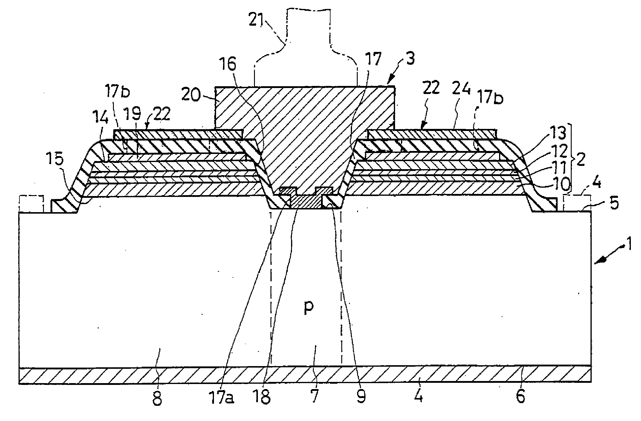
[0097] A pn-junction diode is employed in this embodiment as an overvoltage protector in place of the Schottky barrier diode of the preceding embodiment. An n-type semiconductor region 40 is formed in part of the core section 7 of the substrate 1 for providing the pn-junction diode. All the other details of construction are as set forth above in connection with the FIGS. 1-8 embodiment except for the absence of the Schottky electrode.

[0098] The pn-junction diode is comprised of the p-type semiconductor substrate 1 and n-type semiconductor region 40, forming a pn-junction therebetween. The n-type semiconductor region 40 is created by diffusing an n-type conductivity determinant into the core section 7 of the substrate 1 from its top surface 5.

[0099] The vacancy created by the absence of the Schottky barrier diode of the preceding embodiment is filled by part 18a of the bonding pad 20 which extends through the central opening 17a in the transparent overlay 17 into ohmic con...


PUM


Abstract

An LED comprises a multilayered light-generating semiconductor region grown on one of a pair of opposite major surfaces of a semiconducting silicon substrate, a bonding pad overlying the light-generating semiconductor region and received in part in a cavity formed centrally therein, and a substrate electrode on the other major surface of the substrate. For protecting the LED from voltage spikes or like transients, an overvoltage protector such as a Schottky barrier diode is interposed between the bonding pad and the substrate. Further, for a uniform current distribution throughout the light-generating semiconductor region, a current-spreading film of electrically conducting, optically transparent material overlies the light-generating semiconductor region and itself covered by a transparent overlay of electrically insulating material. The bonding pad is electrically coupled to the current-spreading film via a plurality of connector strips extending radially from the pad over the transparent overlay. The connector strips have ribs depending therefrom and extending through radial slits in the transparent overlay into electrical contact with the current-spreading film.

Description

CROSS REFERENCE TO RELATED APPLICATIONS [0001] This application claims priority to Japanese Patent Application No. 2006-138303, filed May 17, 2006. BACKGROUND OF THE INVENTION [0002] This invention relates to light-emitting semiconductor devices, or light-emitting diodes (LEDs) according to common parlance, and particularly to those monolithically integrated with an overvoltage protector. More particularly, the invention concerns how to improve the light-emitting efficiency of such overvoltage-protected light-emitting semiconductor devices. Overvoltage protectors that can be integrated with light-emitting semiconductor devices according to the invention include, but are not limited to, the Schottky barrier diode, pn-junction diode, varistor, and capacitor. [0003] Japanese Unexamined Patent Publication No. 2000-66863, filed by the assignee of the instant invention, suggests an overvoltage-protected LED of particular pertinence to the present application. It comprises a light-generati...

Claims


Application Information

Patent Timeline
Patent Type & Authority Applications(United States)
IPC IPC(8): H01L33/00H01L33/32H01L33/42H01L33/44
CPCH01L27/15H01L33/382H01L33/42H01L2224/04042H01L2224/05556H01L2224/05555H01L2924/12032H01L24/05H01L2224/48463H01L2924/00H01L2924/12036H01L2924/12041
Inventor SUGIMORI, NOBUHISA
Owner SANKEN ELECTRIC CO LTD
Why Eureka
Try Eureka