Memory system with a retiming circuit and a method of exchanging data and timing signals between a memory controller and a memory device
a memory controller and timing signal technology, applied in the field of memory systems with a controller and a memory device, can solve the problems of increasing the cost, the latency of encryption and decryption, and the cost of encryption and decryption
- Summary
- Abstract
- Description
- Claims
- Application Information
AI Technical Summary
Benefits of technology
Problems solved by technology
Method used
Image
Examples
third embodiment
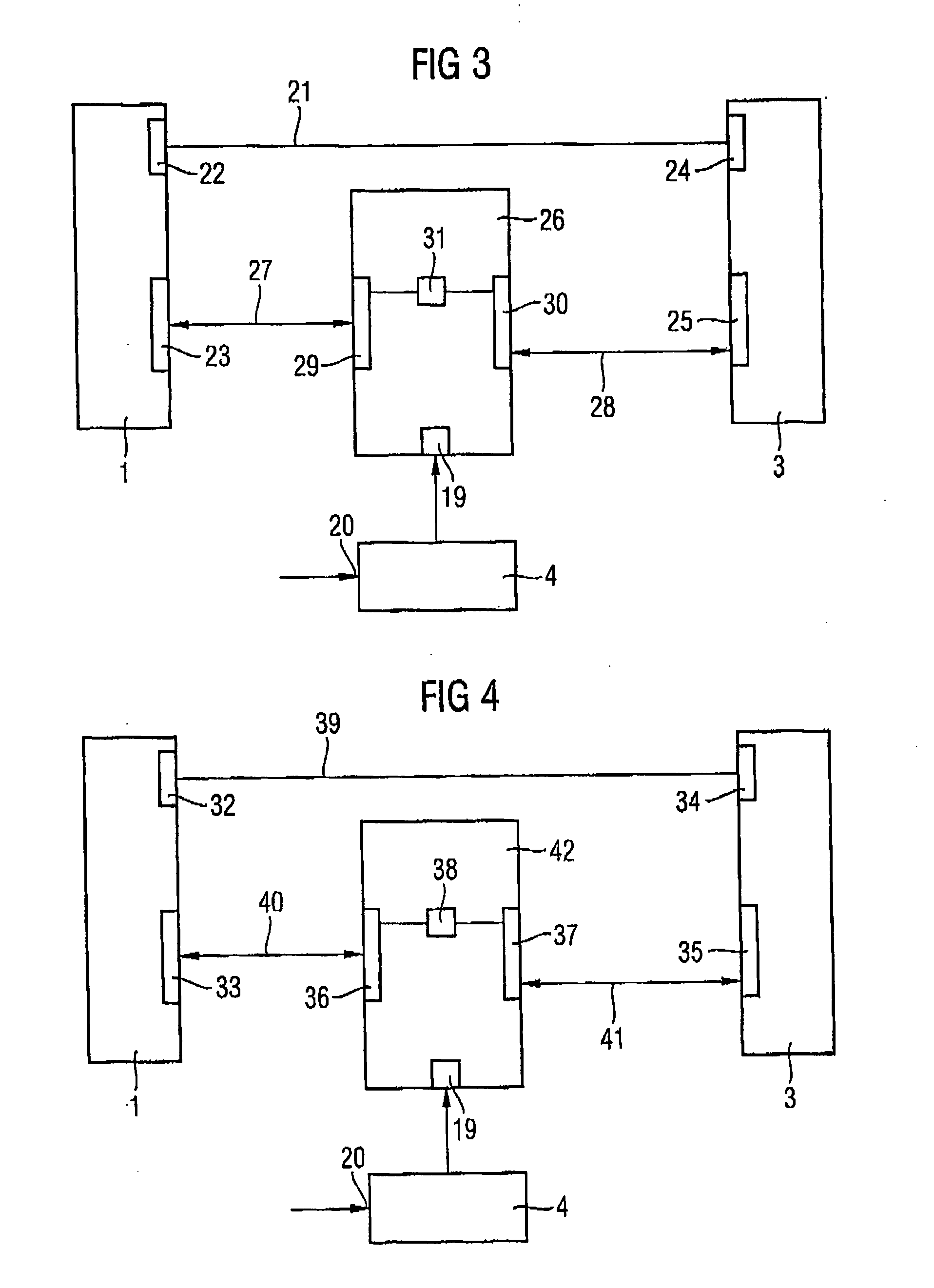
[0041]FIG. 3 depicts a third embodiment with a further data path 21 that is directly guided from the controller 1 to the memory device 3. The controller 1 comprises a further first interface 22 that is connected to the further data path 21. The further data path 21 is connected with a further third interface 24 of the memory device 3. The controller 1 comprises a further second interface 23 that is connected with a further first timing path 27. The further first timing path 27 is connected with a further fifth interface 29 of a further retiming circuit 26. The further retiming circuit 26 comprises a further sixth interface 30 that is connected with a further second timing path 28. The further second timing path 28 is guided to a further fourth interface 25 of the memory device 3.
[0042]The further retiming circuit 26 is connected by an input signal 19 with an arbiter 4. In this embodiment, only the timing path and the timing signals or at least a part of the timing signals are guided...
fourth embodiment
[0044]In a fourth embodiment as shown in FIG. 4, only the information signals or at least a part of the information signals are transferred by a further second retiming circuit 42 from the controller 1 to the memory device 3 and vice versa. The timing signal is guided in this embodiment directly from the controller 1 to the memory device 3. The controller 1 comprises a further seventh interface 32 that is connected with a further third timing path 39. The further third timing path 39 is directly guided from the controller 1 to a further ninth interface 34 of the memory device 3. Furthermore, the controller 1 comprises a further eighth interface 33 that is connected with a further first data path 40. The further first data path 40 is guided to a further eleventh interface 36 of a further second retiming circuit 42. The further second retiming circuit 42 comprises a further second delay circuit 38 that is connected with the further eleventh interface 36 and a further twelfth interface...
PUM
 Abstract
Description
Claims
Application Information


