Semiconductor apparatus design method and execution program therefor

a technology of semiconductor apparatus and design method, which is applied in the direction of instruments, computing, electric digital data processing, etc., can solve the problems of parasitic capacitance increase, signal transmission delay, and breakage of the upper layer, so as to improve the reliability of the semiconductor apparatus and suppress the increase of parasitic capacitance of the signal lin

Active Publication Date: 2007-12-13
RENESAS ELECTRONICS CORP
View PDF16 Cites 11 Cited by
  • Summary
  • Abstract
  • Description
  • Claims
  • Application Information

AI Technical Summary

Benefits of technology

[0013]A semiconductor apparatus and its design method according to the present invention can suppress an increase in parasitic capacitance of a

Problems solved by technology

The multilayered lines have a problem that a line of an upper layer is subject to breaking due to unevenness of a line of a lower layer.
Further, if an area of a metal line is larger, parasitic capacitance increases accordingly.
Therefore, if a large dummy line is placed in close proximity to a signal line, parasitic capacitance of lines increases to cause larger signal transmission delay.
However, the related art 2 has a problem that the number of patterns increases as the number of blocks increases.
Thus, if the number of patterns is large, it takes an enormous amount of time for the OPC process.
Further, an increase in the number of patterns causes an increase in cost for mask production.
If a sig

Method used


Image

  • Semiconductor apparatus design method and execution program therefor
  • Semiconductor apparatus design method and execution program therefor
  • Semiconductor apparatus design method and execution program therefor

Examples


first embodiment

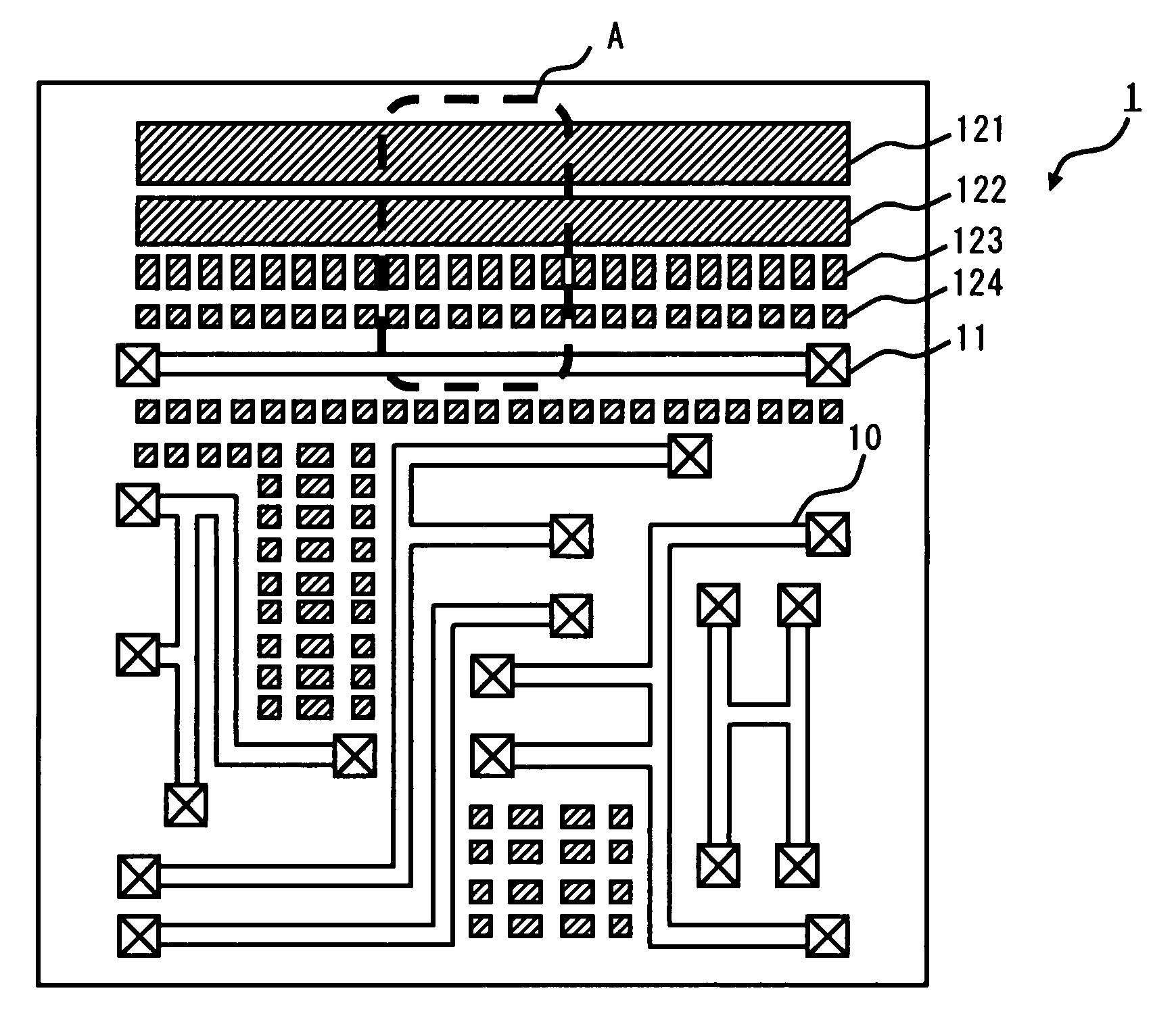
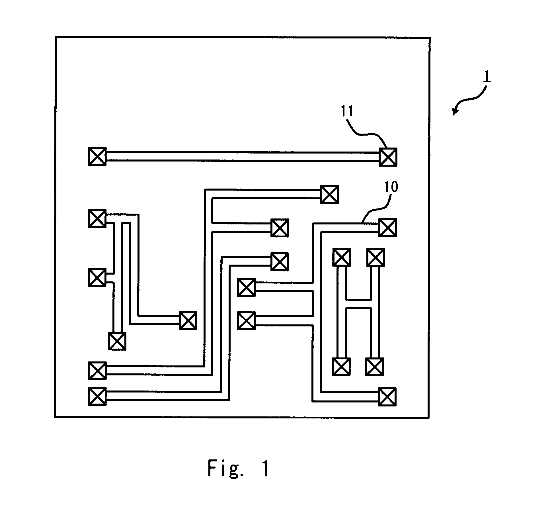
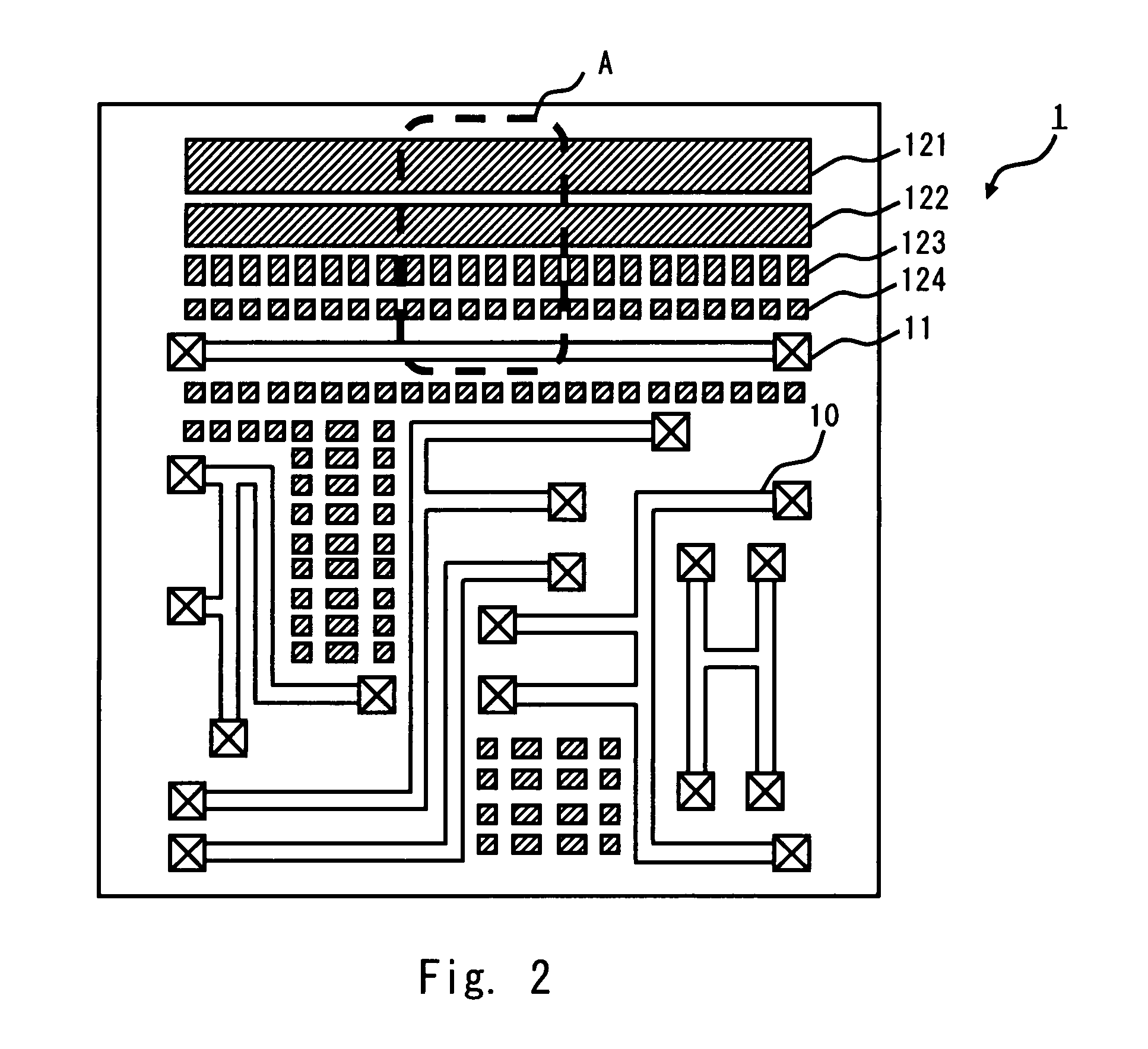
[0024]Exemplary embodiments of the present invention are described hereinafter with reference to the drawings. FIG. 1 schematically shows the layout regarding a metal line layer 1, which is one of metal line layers in a semiconductor apparatus according to a first embodiment of the invention. As shown in FIG. 1, the metal line layer 1 includes a signal line 10 and a via 11. The signal line 10 is a metal line which serves as a transmission path of signals that are processed in the semiconductor apparatus. The via 11 is a connection terminal between the signal line 10 and a device or a line which are placed in another layer.

[0025]In the metal line layer 1 shown in FIG. 1, the pattern density of signal lines differs by area. Thus, in the semiconductor apparatus of this embodiment, a dummy line, which is placed in a “floating state” with no connection to any line, is placed in the area where the pattern density of signal lines is low. FIG. 2 schematically shows the layout where dummy li...

second embodiment

[0041]A semiconductor apparatus 2 according to a second embodiment of the present invention is substantially the same as the semiconductor apparatus 1 according to the first embodiment. In the semiconductor apparatus 1 of the first embodiment, the length a of the side of a divided dummy line which is in parallel with a signal line is equal. On the other hand, in the semiconductor apparatus 2 of the second embodiment, the length a of the side of a divided dummy line which is in parallel with a signal line differs according to a distance from the signal line. FIG. 5 schematically shows the layout of the semiconductor apparatus according to the second embodiment of the invention.

[0042]As shown in FIG. 5, the length of the side of the divided dummy line 123′ which is in parallel with a signal line is longer than the length of the side of the divided dummy line 124 which closer to the signal line than the dummy line 123′. In the second embodiment, the length of the side of a divided dumm...


PUM


Abstract

A design method places a dummy line in floating state in a line layer of a semiconductor apparatus by using a computer. The method includes a first step of reading layout data and placing a dummy line with a longitudinal side lying in parallel with a signal line in an area where a pattern density of the signal line in a prescribed area is equal to or lower than a density lower limit, and a second step of dividing a dummy line placed in an area where a distance from the signal line is equal to or shorter than a dummy dividing distance.

Description

BACKGROUND OF THE INVENTION[0001]1. Field of the Invention[0002]The present invention relates to a method of designing a semiconductor apparatus and, particularly, to a method of designing a semiconductor apparatus in which a dummy line is placed in close proximity to a signal line.[0003]2. Description of Related Art[0004]Recent semiconductor apparatus include multilayered lines. The multilayered lines have a problem that a line of an upper layer is subject to breaking due to unevenness of a line of a lower layer. To address such a problem, there is a technique that equalizes the pattern density of an entire chip for each layer. This technique is disclosed in Japanese Unexamined Patent Application Publication No. 2003-140319 (Related art 1).[0005]FIG. 7 schematically shows the layout of a semiconductor apparatus 100 according to the related art 1. As shown in FIG. 7, the semiconductor apparatus 100 includes a signal line 101 and a dummy line 102. According to the related art 1, if t...

Claims


Application Information

Patent Timeline
IPC IPC(8): G06F17/50
CPCG06F17/5072G06F30/392
Inventor KOBAYASHI, NAOHIRO
Owner RENESAS ELECTRONICS CORP
Why Eureka
Try Eureka