Semiconductor device and method for manufacturing semiconductor device

a semiconductor and semiconductor technology, applied in the direction of solid-state devices, transistors, basic electric elements, etc., can solve the problems of short supply of si substrates, reduced cost, and inability to read shields, so as to achieve certain communication distances and improve signal processing speed.

Inactive Publication Date: 2007-12-20
SEMICON ENERGY LAB CO LTD
View PDF60 Cites 10 Cited by
  • Summary
  • Abstract
  • Description
  • Claims
  • Application Information

AI Technical Summary

Benefits of technology

[0019] Circuits and capacitor elements are formed using a semiconductor film of a large grain crystal region formed by laser light irradiation, so that higher signal processing speed is realized and a certain communication distance can be ensured.

Problems solved by technology

At present, product management using barcodes or the like is a mainstream; however, since data of barcodes are read optically, they cannot be read when a shield exists.
However, in the case of manufacturing a semiconductor device using a single crystal Si substrate, since a single crystal Si substrate is expensive, reduction in cost is limited.
In addition, Si substrates are used in different fields so that there are concerns of the short supply of Si substrates if a great number of Si substrates are used.
Therefore, when a single crystal Si substrate is used, cost reduction is more difficult.
However, there are problems in that the processing speed, communication distance, and the like depend on a crystal state of the semiconductor thin film formed over a substrate, or the layout of circuits formed using the semiconductor thin film or the like, for example.

Method used


Image

  • Semiconductor device and method for manufacturing semiconductor device
  • Semiconductor device and method for manufacturing semiconductor device
  • Semiconductor device and method for manufacturing semiconductor device

Examples


embodiment mode 1

[0032] In this embodiment mode, a semiconductor device of the present invention will be described with respect to drawings.

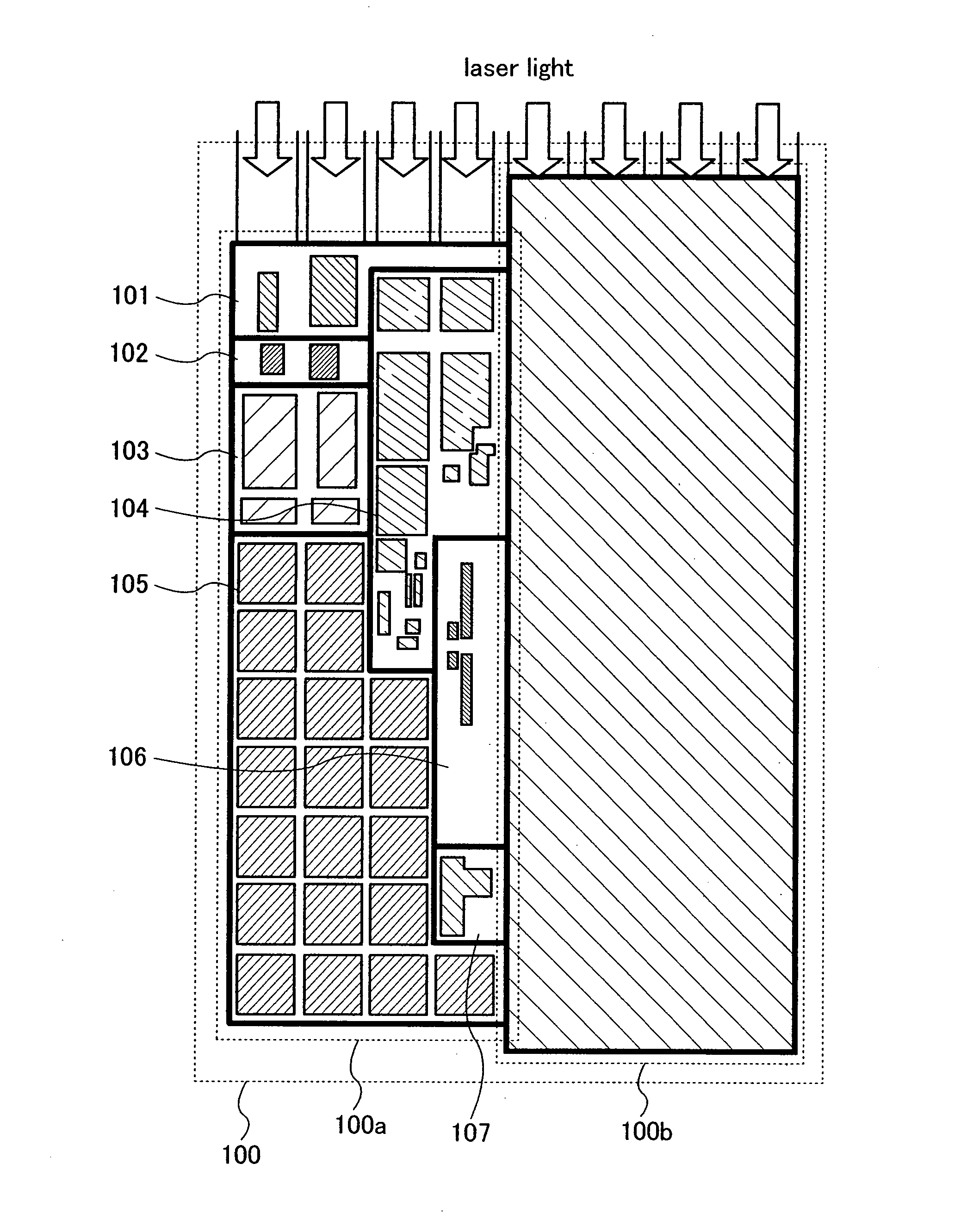
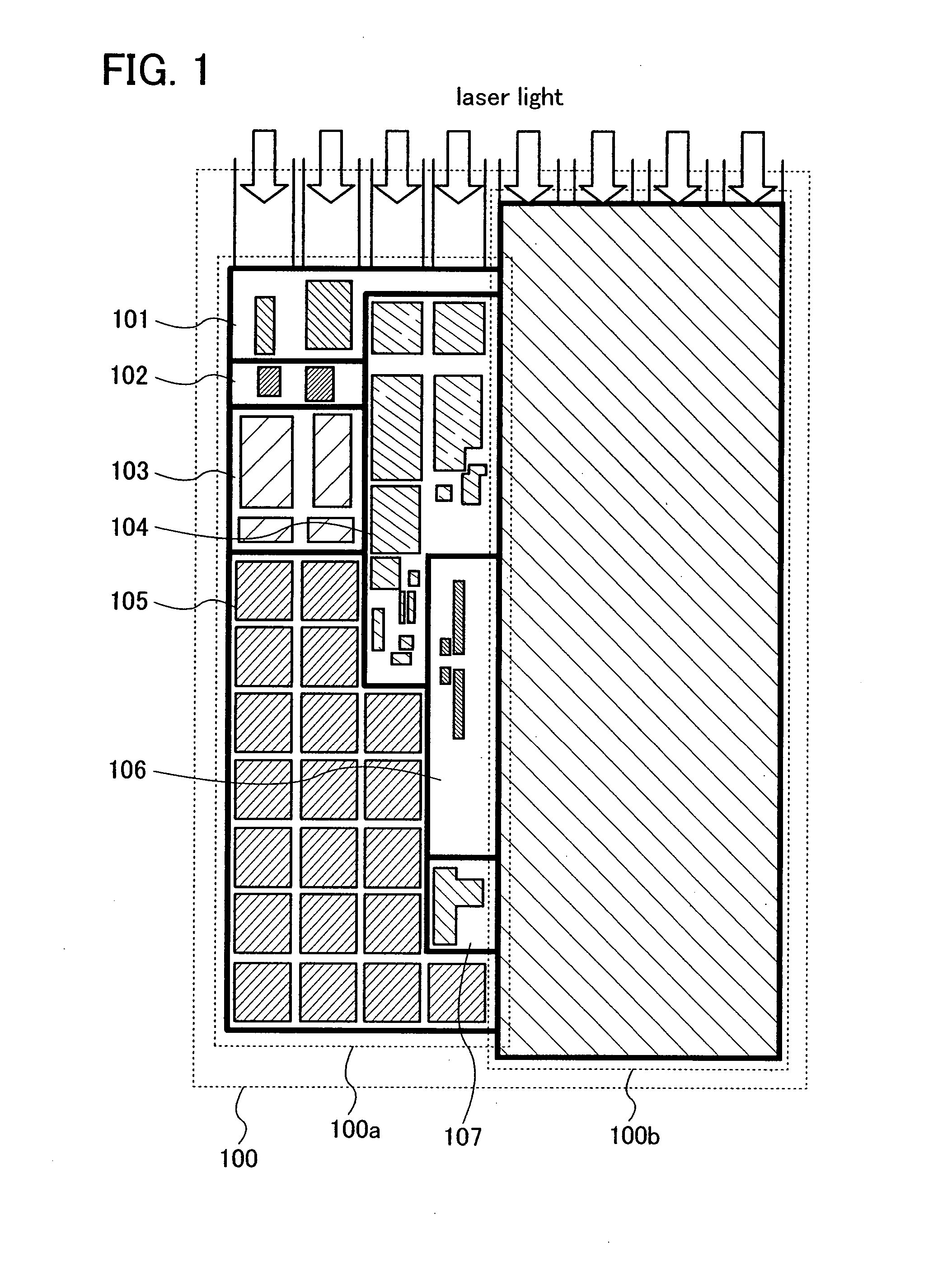
[0033] A semiconductor device 100 of the invention includes an analog circuit portion 100a and a digital circuit portion 100b. The analog circuit portion 100a and the digital circuit portion 100b are provided to be separated from each other (See FIG. 1). The analog circuit portion 100a includes a demodulation circuit 101, a modulation circuit 102, a rectification circuit 103, a constant voltage circuit 104, a capacitor portion 105, an oscillator circuit 106, a reset circuit 107, and the like. The digital circuit portion 100b includes a memory portion, a memory circuit, and the like.

[0034] Further, circuits formed in the analog circuit portion 100a and the digital circuit portion 100b includes thin film transistors or the like formed over a substrate. The capacitor portion 105 is provided with a plurality of capacitor elements manufactured using the semiconduct...

embodiment mode 2

[0063] This embodiment mode will describe an example of a method for manufacturing a semiconductor device of the present invention with reference to drawings.

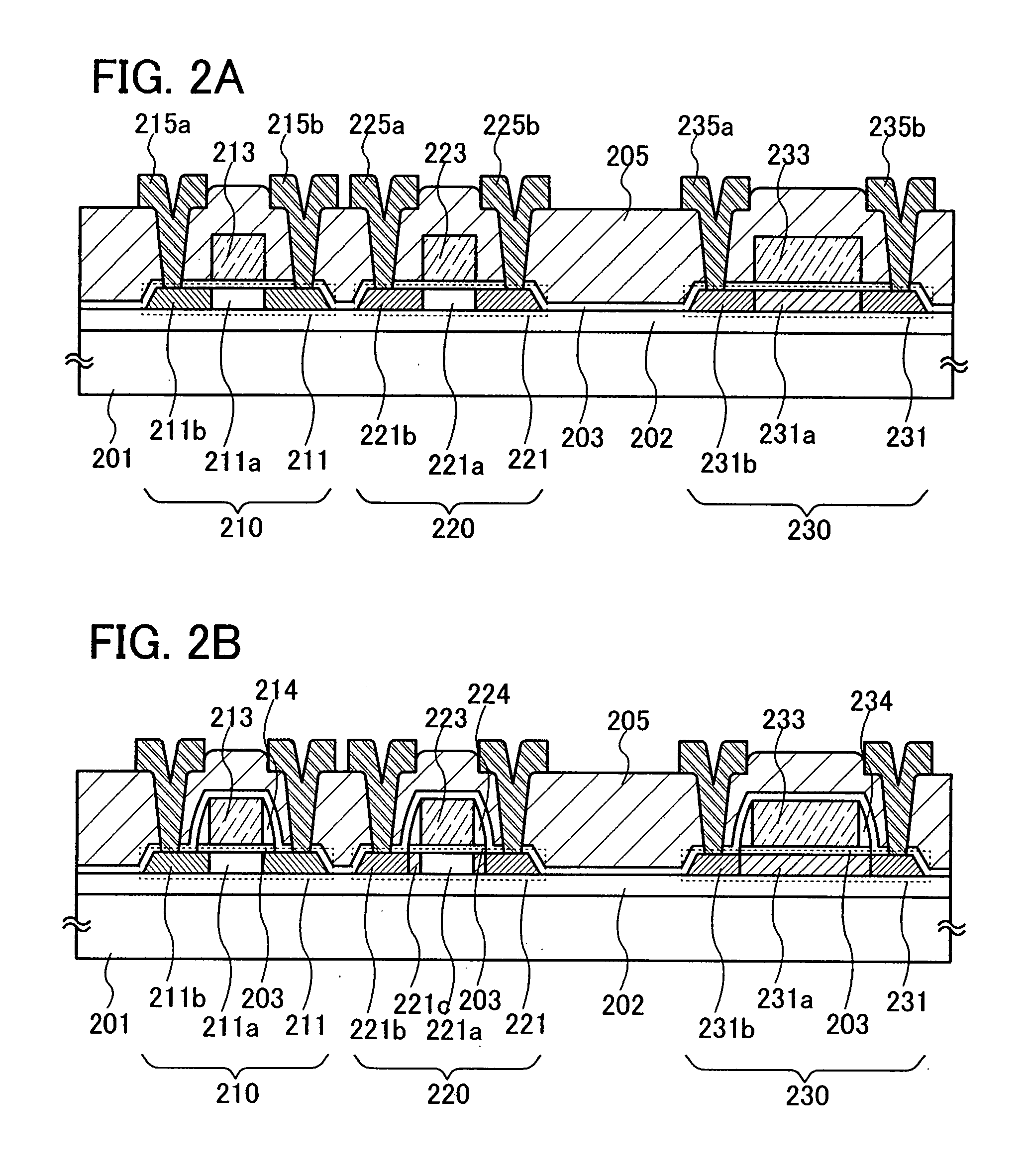
[0064] First, a semiconductor film 403 is formed over a substrate 401 with an insulating film 402 therebetween. Further, regions with grains having large grain sizes, 403a are formed in the semiconductor film 403 by irradiating the semiconductor film 403 with laser light (FIG. 7A). Poor crystallinity regions 403b are formed at end portions of the regions with grains having large grain sizes, 403a.

[0065] The substrate 401 is selected from a glass substrate, a quartz substrate, a metal substrate (for example, a stainless-steel substrate or the like), a ceramic substrate, a semiconductor substrate such as a Si substrate, and the like. Alternatively, a plastic substrate such as a substrate of polyethylene terephthalate (PET), polyethylene naphthalate (PEN), polyethersulfone (PES), or acrylic can be selected.

[0066] The insulating...

embodiment mode 3

[0092] In this embodiment mode, an example of a semiconductor device of the present invention will be described with reference to drawings. Specifically, a semiconductor device provided with a PLL (Phase Locked Loop) circuit portion will be described with reference to drawings.

[0093]FIG. 9 is a block diagram showing one exemplary configuration of a semiconductor device which can perform transmission / reception of instructions or data with radio signals. This semiconductor device includes an antenna portion 902, an RF circuit portion 903, a power supply circuit portion 905, and a logic circuit portion 907. The antenna portion 902 communicates signals with a communication device which is also called a reader / writer. Frequencies of carrier waves for delivering signals can be LF bands (1 to 135 kHz), HF bands (6.78 MHz, 13.56 MHz, 27.125 MHz, 40.68 MHz, or 5.0 MHz), microwave bands (2.45 GHz, 5.8 GHz, or 24.125 GHz), or the like. The antenna portion 902 can have either a coiled shape, m...


PUM


Abstract

In a semiconductor device including a digital circuit portion and an analog circuit portion having a capacitor portion provided over a substrate, the capacitor portion is provided with a first wiring, a second wiring and a plurality of blocks each having a plurality of capacitor elements. Further, each the plurality of capacitor elements provided in each block has a semiconductor film having a first impurity region and a plurality of second impurity regions provided apart with the first impurity region interposed therebetween, and a conductive film provided over the first impurity region with an insulating film therebetween. A capacitor is formed from the first impurity region, the insulating film, and the conductive film.

Description

BACKGROUND OF THE INVENTION [0001] 1. Field of the Invention [0002] The present invention relates to a semiconductor device and a method for manufacturing the semiconductor device, particularly, a method for manufacturing a semiconductor device using a thin film transistor. [0003] 2. Description of the Related Art [0004] In recent years, IT (Information Technology) penetrates the world due to the propagation of the Internet, which has brought revolution. In particular, as expressed as a ubiquitous information society, nowadays, the environment making it possible to access networks everywhere at any time has been developed. In such an environment, individual verification technologies attract attention, in which an ID (identification code) is assigned to an individual object thereby specifying the history of the object and it is applied to production, management, or the like. [0005] Among them, currently, a semiconductor device in which a micro IC chip manufactured using a single crys...

Claims


Application Information

Patent Timeline
Patent Type & Authority Applications(United States)
IPC IPC(8): H01L29/94H01L21/20
CPCH01L21/2026H01L27/1255H01L28/40H01L27/1296H01L27/1285H01L21/02532H01L21/02683H01L21/02686H01L23/50H01L23/58
Inventor ATSUMI, TOMOAKIINOUE, HIROKI
Owner SEMICON ENERGY LAB CO LTD
Why Eureka
Try Eureka