Radio frequency switching circuit, radio frequency switching device, and transmitter module device

a radio frequency switching and radio frequency technology, applied in electronic switching, semiconductor devices, pulse techniques, etc., can solve the problems of difficult to overcome deterioration of radio frequency characteristics, and difficulty in overcoming the surge problems of radio frequency switching devices, etc., to achieve desirable radio frequency characteristics and endurance. desirable

Inactive Publication Date: 2007-12-20
PANASONIC CORP
View PDF8 Cites 71 Cited by
  • Summary
  • Abstract
  • Description
  • Claims
  • Application Information

AI Technical Summary

Benefits of technology

[0013]Therefore, an object of the present invention is to provide an inexpensive radio frequency switching circuit having desirable radio frequency characteristics over a wide band, an

Problems solved by technology

However, the configuration of the conventional radio frequency switching circuit 100 requires DC cut capacitors (C11 to C13, Cg1 and Cg2), and the radio frequency characteristics are deteriorated due to the influence of the frequency characteristics of the DC cut capacitors.
In a case where MIM capacitors are formed as DC cut capacitors on the same semiconductor chip with the FETs in the conventional radio frequency switching circuit 100, since an MIM capacitor has a low ESD resistance (electrostatic resistance), th

Method used


Image

  • Radio frequency switching circuit, radio frequency switching device, and transmitter module device
  • Radio frequency switching circuit, radio frequency switching device, and transmitter module device
  • Radio frequency switching circuit, radio frequency switching device, and transmitter module device

Examples


first embodiment

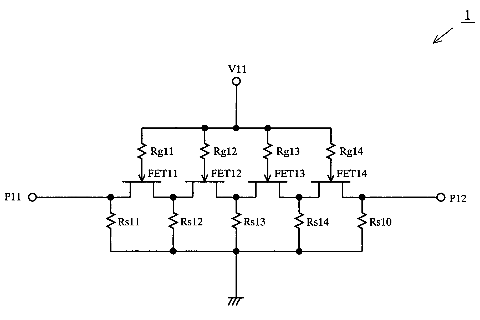
[0036]FIG. 1 shows a configuration of a radio frequency switching circuit 1 according to a first embodiment of the present invention. Referring to FIG. 1, the radio frequency switching circuit 1 includes FETs 11 to 14, and resistors Rg11 to Rg14 and Rs10 to Rs14. The FETs 11 to 14 may be depletion type metal-semiconductor field effect transistors (MES-FETs) whose primary material is gallium arsenide (GaAs), or metal-insulator-semiconductor field effect transistors (MIS-FETs) such as MOS-FETs.

[0037]The FETs 11 to 14 are connected together in series. The source of the FET 11 is connected to the first input / output terminal P11. The drain of the FET 14 is connected to the second input / output terminal P12. The sources and the drains of the FETs 11 to 14 are grounded via the resistors Rs10 to Rs14 each having a predetermined resistance value. The gates of the FETs 11 to 14 are connected to the control terminal V11 via the resistors Rg11 to Rg14, respectively. The first input / output termin...

second embodiment

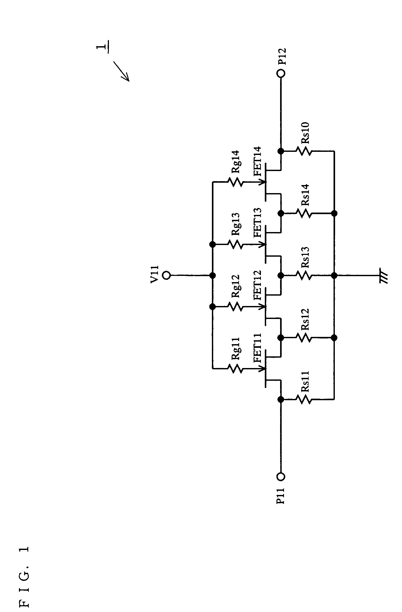
[0044]FIG. 2 shows a configuration of a radio frequency switching circuit 2 according to a second embodiment of the present invention. Referring to FIG. 2, the radio frequency switching circuit 2 includes FETs 15 to 18, and resistors Rg15 to Rg18 and Rs15 to Rs18. The FETs 15 to 18 may be MES-FETs, MIS-FETs, or the like.

[0045]The FETs 15 to 18 are connected together in series. The source of the FET 15 is connected to the first input / output terminal P11 and the second input / output terminal P12. The drain of the FET 18 is grounded. The sources and the drains of the FETs 15 to 18 are grounded via the resistors Rs15 to Rs18, respectively, having a predetermined resistance value. The gates of the FETs 15 to 18 are connected to the control terminal V12 via the resistors Rg15 to Rg18, respectively. The first input / output terminal P11 and the second input / output terminal P12 are each connected to an external circuit such as an antenna circuit or a receiver circuit. A predetermined external ...

third embodiment

[0050]FIG. 3 shows a configuration of a radio frequency switching circuit 3 according to a third embodiment of the present invention. Referring to FIG. 3, the radio frequency switching circuit 3 includes FETs 11 to 18, and resistors Rg11 to Rg18 and Rs11 to Rs18. As can be seen from FIG. 3, the radio frequency switching circuit 3 of the third embodiment is a circuit obtained by combining the radio frequency switching circuit 1 of the first embodiment as a transfer circuit section with the radio frequency switching circuit 2 of the second embodiment as a shunt circuit. The resistor Rs10 is omitted since the resistor Rs15 serves as a shared resistor. It is understood that the number of FETs connected together in series in the transfer circuit section or the shunt circuit section.

[0051]Consider a case where an actuating voltage of 0V is applied to the control terminal V11, and a non-actuating voltage of −3V is applied to the control terminal V12. In such a case, each of the FETs (FETs ...


PUM


Abstract

The present invention provides an inexpensive radio frequency switching circuit having desirable radio frequency characteristics over a wide band and desirable endurance against the inflow of a high voltage signal such as an electrostatic surge. Either a negative bias voltage or a positive bias voltage being greater than or equal to 0V and less than or equal to a Schottky forward voltage is used for the control terminals V11 and V12 for controlling FETs 11 to 18 and FETs 21 to 28 so as to turn ON/OFF the path extending from the first input/output terminal P11 to the second input/output terminal P12 and the path extending from the first input/output terminal P11 to the third input/output terminal P13. Thus, it is possible to eliminate the need for DC cut capacitors.

Description

BACKGROUND OF THE INVENTION[0001]1. Field of the Invention[0002]The present invention relates to a radio frequency switching circuit for switching between a plurality of signal paths in a mobile communications device, or the like, and to a radio frequency switching device and a transmitter module device including such the radio frequency switching circuit combined with a negative bias generation device.[0003]2. Description of the Background Art[0004]In recent years, along with the increase in the functionalities of mobile communications devices, there are strong demands for reducing the size of, and increasing the functionalities of, radio frequency devices for use in terminal devices. Particularly, radio frequency switching devices for switching between antennas are required to achieve low loss characteristics.[0005]FIG. 14 shows an exemplary equivalent circuit of a SPDT (Single-Pole Double-Throw) switching device, being an example of a conventional radio frequency switching device...

Claims


Application Information

Patent Timeline
IPC IPC(8): H03F1/14
CPCH03F3/24H03K17/693H03K2017/6875H03K17/102H01L2924/0002H03K2217/0054H01L2924/00
Inventor ADACHI, MASAKAZUNAKATSUKA, TADAYOSHI
Owner PANASONIC CORP
Why Eureka
Try Eureka