Structure of pixel circuit for display and driving method thereof

a technology of pixel circuit and driving method, which is applied in the direction of instruments, static indicating devices, etc., can solve the problems of shortened device lifetime, low cost, and harm to the eyes of viewers, and achieve the effect of reducing the fabricating cost extending the lifetime of the display panel, and increasing the pixel aperture ratio of the display panel

Inactive Publication Date: 2007-12-20
AU OPTRONICS CORP
View PDF5 Cites 29 Cited by
  • Summary
  • Abstract
  • Description
  • Claims
  • Application Information

AI Technical Summary

Benefits of technology

[0037]According to the present invention, the coupling effect of the coupling capacitor is adopted for compensating the threshold voltage of the second transistor, and further the driving current for driving the luminescent element can be sustained, so that the brightness of the luminescent element is not affected by drift of the threshold voltage. Moreover, compensation to the threshold voltage of the second transistor is achieved with only two thin film transistors and one coupling capacitor in the entire pixel circuit, and furthermore, the pixel aperture ratio of the display panel is increased, the fabricating cost of the display panel is reduced, and the lifetime of the display panel is extended.

Problems solved by technology

Even though traditional cathode ray tube (CRT) display still has the advantage of lower cost, such display is too bulky, and the radiation produced by a CRT display may harm the viewer's eyes.
The passive matrix OLED has a simple structure, thus the cost thereof is low; however, the disadvantage of the passive matrix OLED is that such OLED is not suitable for displaying high resolution images, and the problems of increased power consumption, shortened device lifetime, and bad display performance will be caused when such OLED is developed towards large-sized panel.
Active matrix OLED has such outstanding advantages as broad view angle, high brightness, and fast response time besides being applied to large-sized active matrix driving; however, the fabricating cost thereof is slightly higher than that of the passive matrix OLED.
However, new circuits and ICs need to be developed for such method of current driving pixel, and thus the cost thereof is very high.
However, when driving OLEDs with the voltage driving circuit of TFT-LCD, drift of the threshold voltage of the driving thin film transistor may be caused after operating for a long time, and accordingly the threshold voltage will increases gradually.
As a result, the lifetime of the display panel is shortened.
However, the characteristic of the inverter composed of a single thin film transistor 201 is not very ideal, and the definition of the grey scales of the display panel has to be considered additionally. FIG. 3 illustrates another pixel circuit for compensating threshold voltage.
The fabricating cost will be increased if polysilicon process is adopted to avoid the aperture ratio being affected by the number of transistors or if the foregoing inverter driving principle is used for compensating the threshold voltage.

Method used


Image

  • Structure of pixel circuit for display and driving method thereof
  • Structure of pixel circuit for display and driving method thereof
  • Structure of pixel circuit for display and driving method thereof

Examples


Embodiment Construction

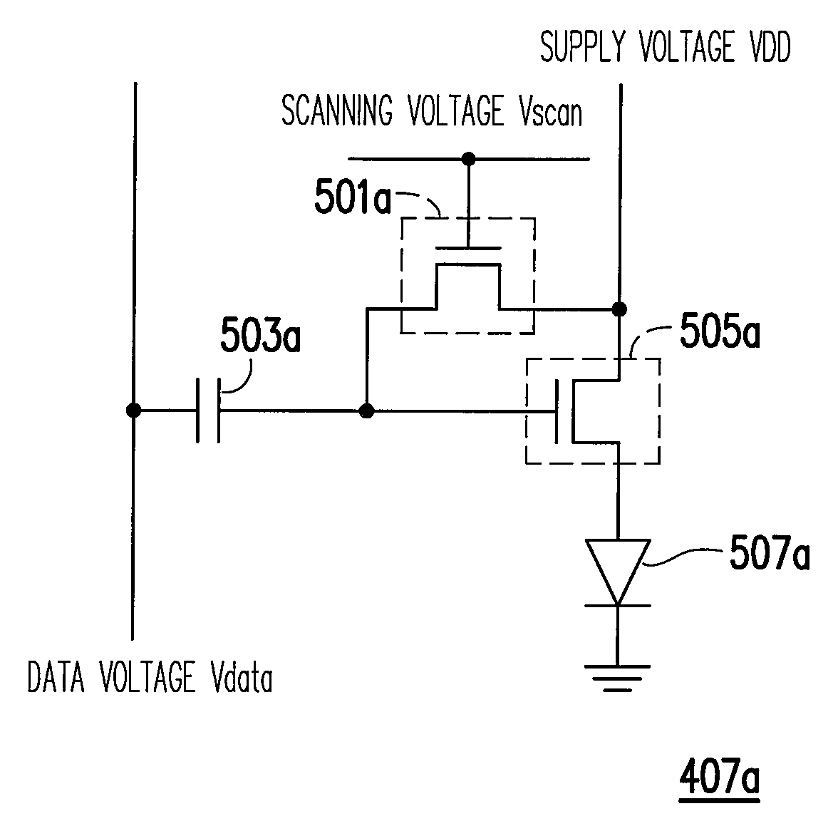
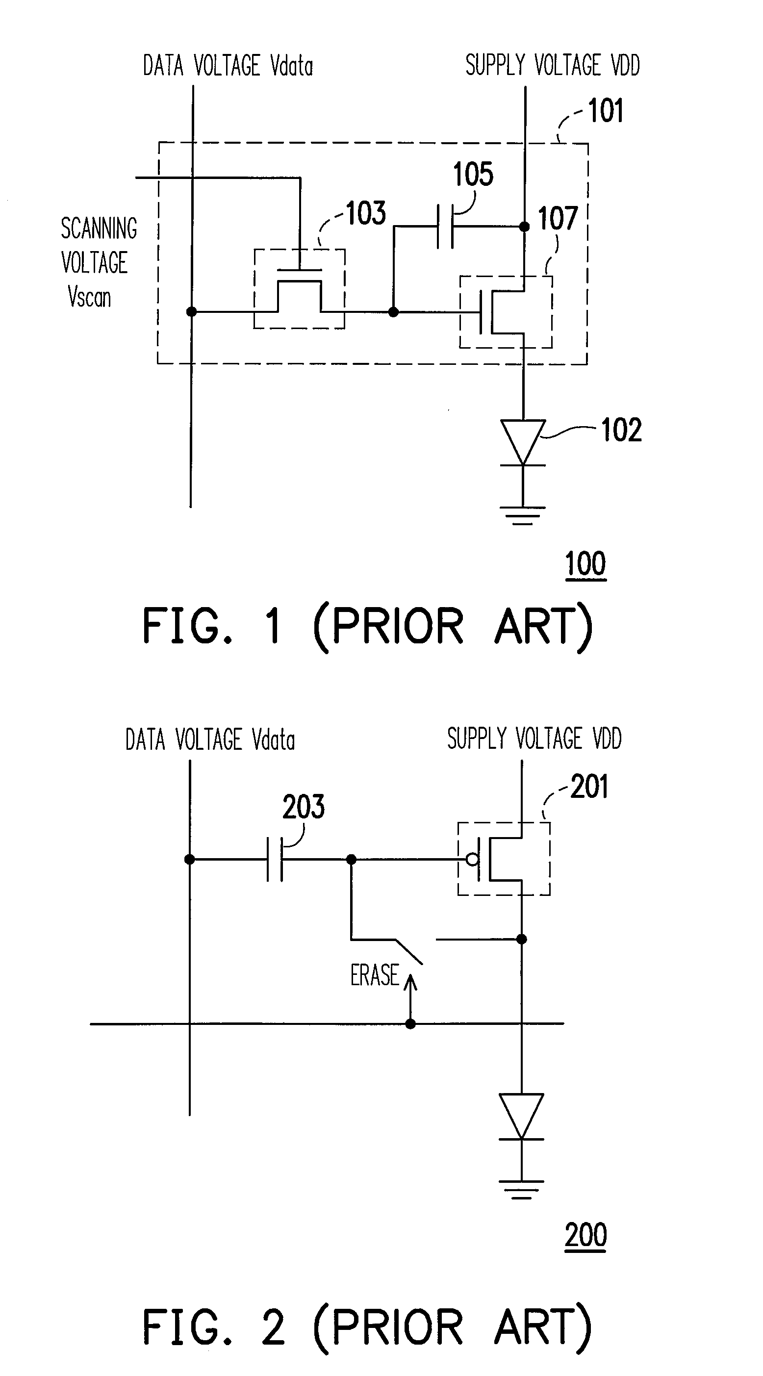
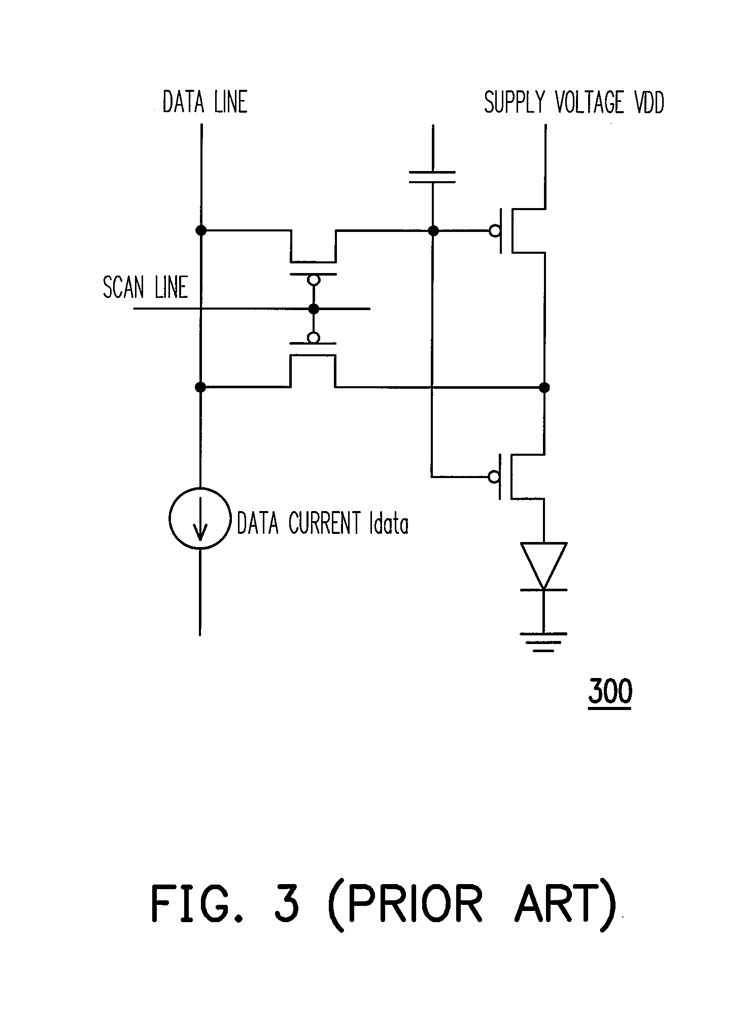
[0053]In conventional technology, a drift of the threshold voltage of the driving thin film transistor may be caused when the driving thin film transistor works for a long time, which may further reduce the driving current produced by the driving transistor, and to sustain the required driving current, more than three transistors are required in the pixel circuit, which may reduce the pixel aperture ratio of the display panel, accordingly the brightness of the display panel may be reduced in both cases. To resolve the foregoing problems, the present invention provides a pixel circuit, a display, and a method for driving a display panel.

[0054]FIG. 4 illustrates a display according to an embodiment of the present invention. Referring to FIG. 4, the display 400 includes a gate driving device 401, a source driving device 403, a system switch 405, and a display panel 407. The gate driving device 401 has a plurality of gate lines G1-Gm for receiving a basic timing, and the gate driving de...


PUM


Abstract

A pixel circuit including a first transistor, a coupling capacitor, a second transistor, and a luminescent element is provided. The first transistor is used as a switch. The coupling capacitor stores a coupling voltage and transmits the coupling voltage to the gate of the second transistor for compensating a drift of the threshold voltage of the second transistor. The second transistor provides a driving current for driving the luminescent element to emit light.

Description

CROSS-REFERENCE TO RELATED APPLICATION[0001]This application claims the priority benefit of Taiwan application serial no. 95121183, filed Jun. 14, 2006. All disclosure of the Taiwan application is incorporated herein by reference.BACKGROUND OF THE INVENTION[0002]1. Field of the Invention[0003]The present invention relates to the structure of a pixel circuit and a driving method thereof. More particularly, the present invention relates to the structure of a pixel circuit for a display and a driving method thereof.[0004]2. Description of Related Art[0005]Nowadays the transmission of image information has mostly transformed from analog transmission into digital transmission along with the rapid development of computer performance and the evolvement of the Internet and multimedia technology. Video or image devices are becoming more and more light-weighted and slim-sized to meet the modern life style. Even though traditional cathode ray tube (CRT) display still has the advantage of lower...

Claims


Application Information

Patent Timeline
Patent Type & Authority Applications(United States)
IPC IPC(8): G09G3/36
CPCG09G3/3233G09G2300/043G09G3/3291G09G3/3283
Inventor WEI, YEN-LIN
Owner AU OPTRONICS CORP
Why Eureka
Try Eureka