

Slurry for CMP of Cu film, polishing method and method for manufacturing semiconductor device
a technology of polishing method and cu film, which is applied in the direction of manufacturing tools, lapping machines, other chemical processes, etc., can solve the problems of increasing the quantity of polishing in the second polishing, increasing the difficulty of minimizing the dishing or corrosion of cu film, and increasing the difficulty of cu film corrosion
- Summary
- Abstract
- Description
- Claims
- Application Information
AI Technical Summary
Problems solved by technology
Method used
Image

Examples
embodiment 1
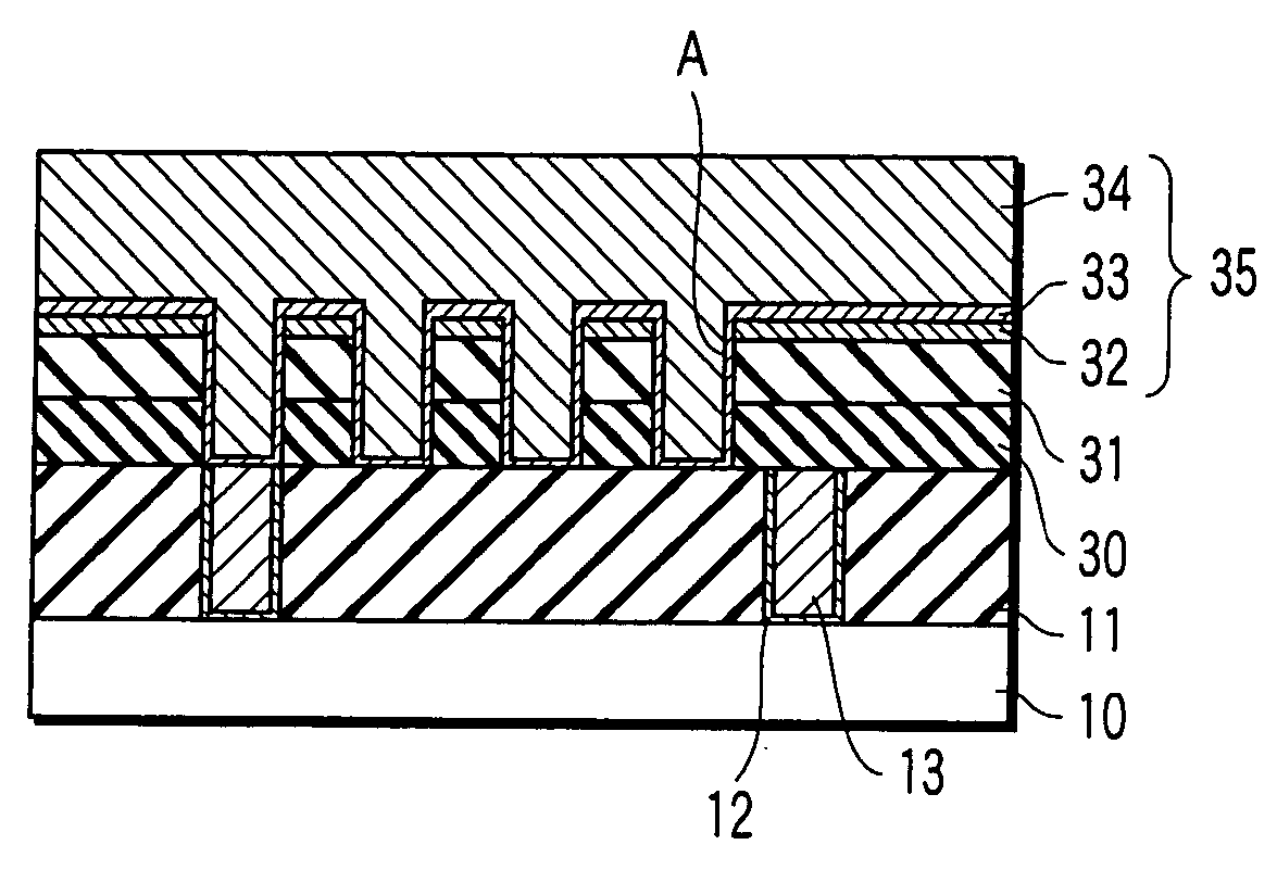
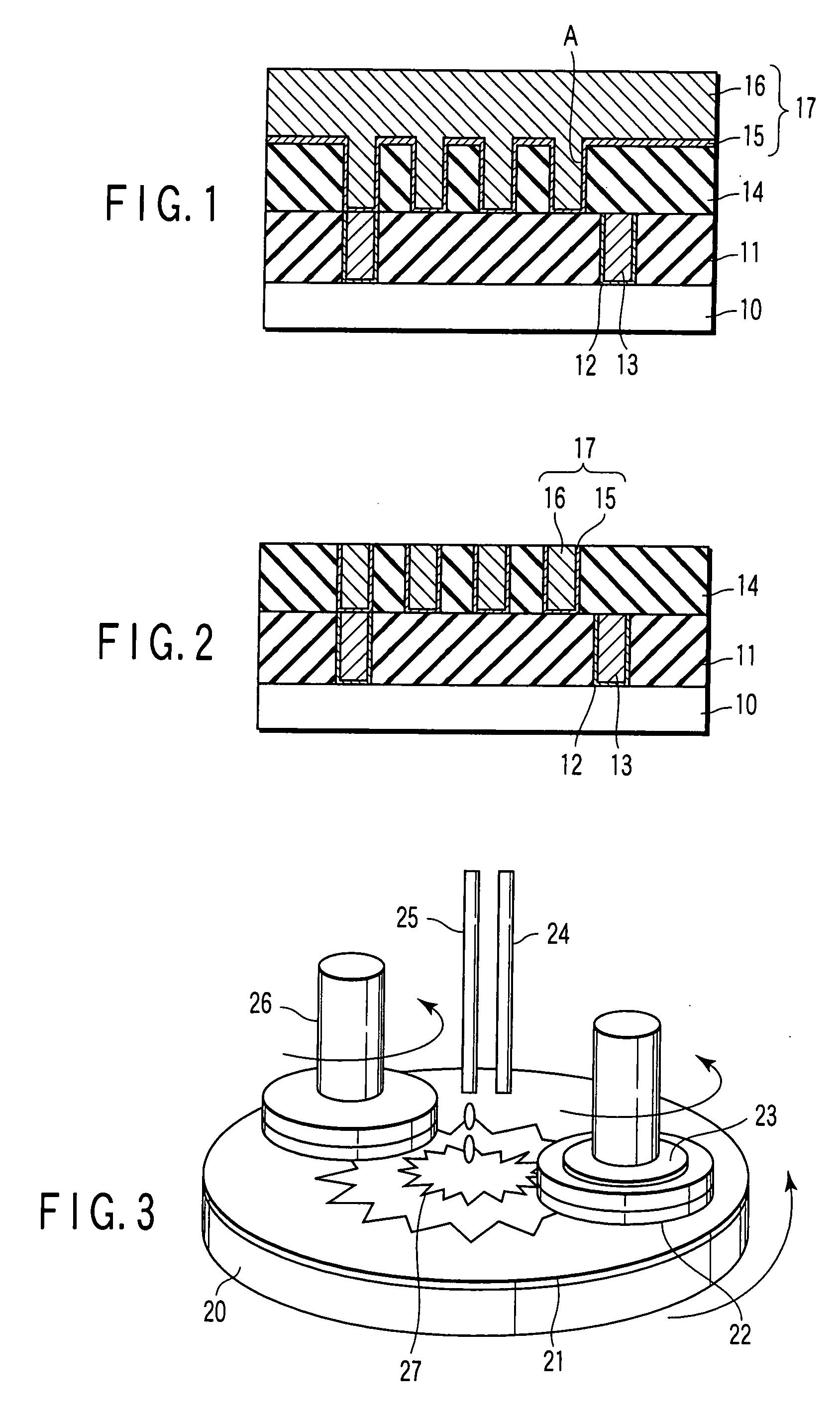
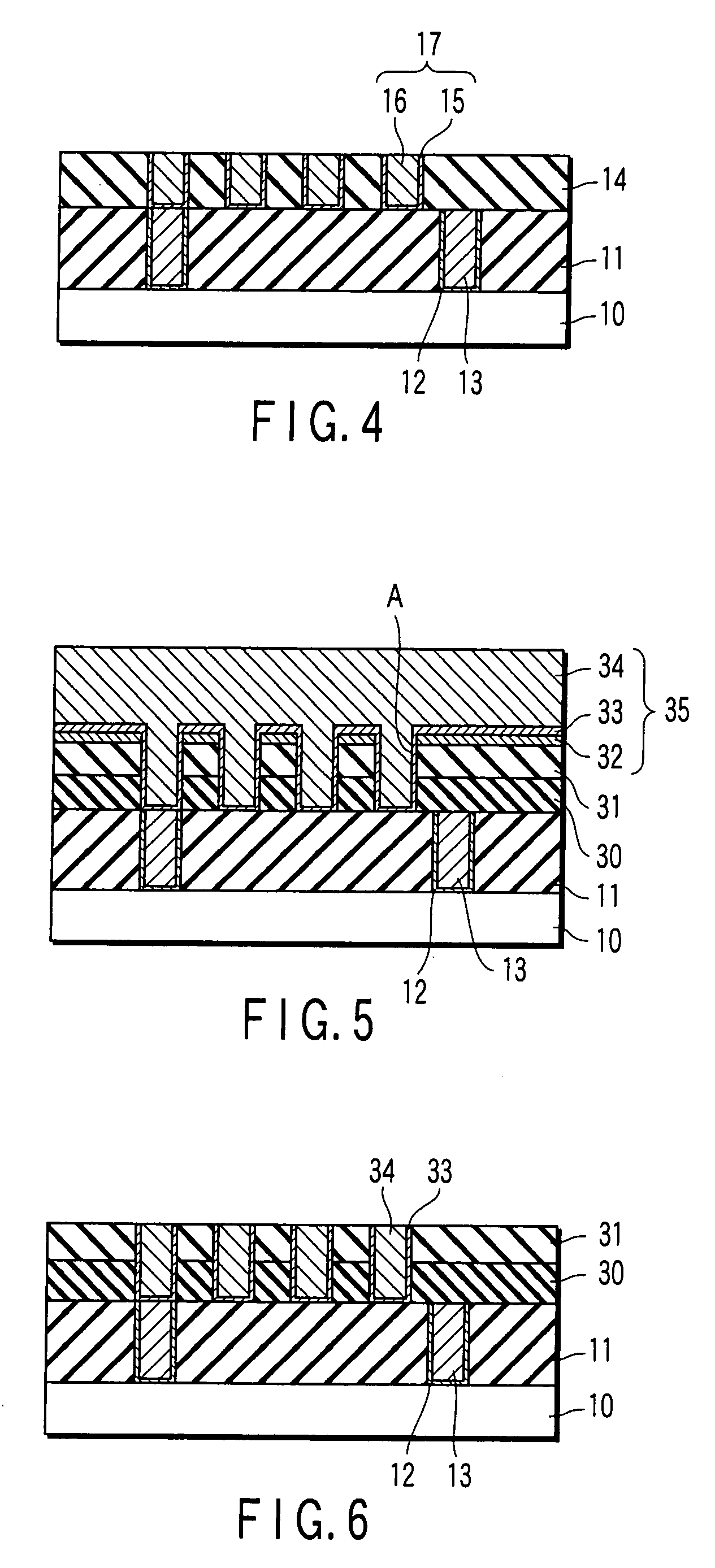
[0054] Embodiment 1 will be explained with reference to FIGS. 1 and 2.
[0055] First of all, as shown in FIG. 1, an insulating film 11 formed of SiO2 was deposited on a semiconductor substrate 10 having semiconductor elements (not shown) formed therein and then a plug 13 was formed in the insulating film 11 with a barrier metal 12 being interposed therebetween. The barrier metal 12 was formed by TiN, and the plug 13 was formed by W. Then, a low dielectric constant insulating film 14 was deposited all over the resultant surface.
[0056] The low dielectric constant insulating film 14 can be formed by at least one insulating material selected, for example, from the group consisting of SiC, SiCH, SiCN, SiOC and SiOCH. In this embodiment, the low dielectric constant insulating film 14 was formed by SiOC.
[0057] Then, a wiring trench “A” having a width of 60 nm was formed as a recess in the low dielectric constant insulating film 14. Thereafter, a Ti film having a thickness of 2 nm and func...
embodiment 2
[0103] A structure as shown in FIG. 1 was obtained, wherein the width and intervals of the wiring trench “A” were both set to 65 nm. In this embodiment, in order to investigate the influence of the short by the residue of Cu, a barrier metal 15 was formed by a Ta film having a thickness of 15 nm. The Cu film 16 was removed by CMP to expose the surface of the barrier metal 15. As the slurry, the samples of Nos. 4, 8, 14, 2, 20, 31 and 39 were employed for performing the CMP under the same conditions as in the case of Embodiment 1.
[0104] The surface of the Cu film was observed using a defective-evaluating apparatus (KLA; Tenchol Co., Ltd.) and evaluated based on the existence or non-existence of Cu residue per cm2 according to the following criterions.
[0105]◯: There was no Cu residue
[0106]×: Existence of Cu residue was confirmed
[0107] The results obtained from each of these slurries are summarized in the following Table 13.
[0108] Then, the kind of slurry was changed and CMP was r...
embodiment 3
[0122] On the occasion of forming a trench to be filled with a Cu film by the RIE work in an insulating film having a relative dielectric constant of 3 or less, a mask material constituted by an insulating film made of SiN or SiO2 is employed. In this case, the RIE selectivity ratio would be around 5. When a metal film is employed as a mask material, the RIE selectivity ratio can be enhanced to 10 or more. In this case, since the thin film of mask material can be further made thinner, it is advantageous in the fine working thereof. With respect to the polishing rate on the occasion of the CMP of Cu film, a metal film can be polished at a higher rate as compared with an insulating film such as SiN or SiO2, the metal film can be easily removed. Because of this, it is possible, through the employment of a metal film as a mask material, to perform the polishing which makes it possible to reduce the polishing load and the concentration of abrasive grains and to minimize the mechanical st...
PUM
| Property | Measurement | Unit |
|---|---|---|
| Diameter | aaaaa | aaaaa |
| Speed | aaaaa | aaaaa |
| Speed | aaaaa | aaaaa |
Abstract
Description
Claims
Application Information