Electronic structures utilizing etch resistant boron and phosphorus materials and methods to form same

a technology of boron and phosphorus, applied in the field of dielectric, can solve the problems of poor etch selectivity between the ild layer and the increase of signal delay of ulsi electronic devices

Inactive Publication Date: 2007-12-27
GLOBALFOUNDRIES INC
View PDF11 Cites 13 Cited by
  • Summary
  • Abstract
  • Description
  • Claims
  • Application Information

AI Technical Summary

Benefits of technology

[0014]In one embodiment of the present invention, a BEOL interconnect structure that is robust and tolerant of the problem commonly encountered in BEOL structure fabrication called the “misaligned via” is provided. By “robust” it is meant that during fabrication of the BEOL interconnect structure of the present invention, a via formed on a second metal level may be slightly misaligned with respect to the first metal level below. In a normal prior art structure, when dilute HF cleaning of the via is done, there is damage to

Problems solved by technology

This combined effect increases signal delays in ULSI electronic devices.
A significant problem encountered in forming these BEOL interconnect structures with smaller and smaller dimensions is the etch selectivity is poor between the ILD layer comprised of Si, C, O, and H and the underlying layer.
Another p

Method used


Image

  • Electronic structures utilizing etch resistant boron and phosphorus materials and methods to form same
  • Electronic structures utilizing etch resistant boron and phosphorus materials and methods to form same
  • Electronic structures utilizing etch resistant boron and phosphorus materials and methods to form same

Examples


Embodiment Construction

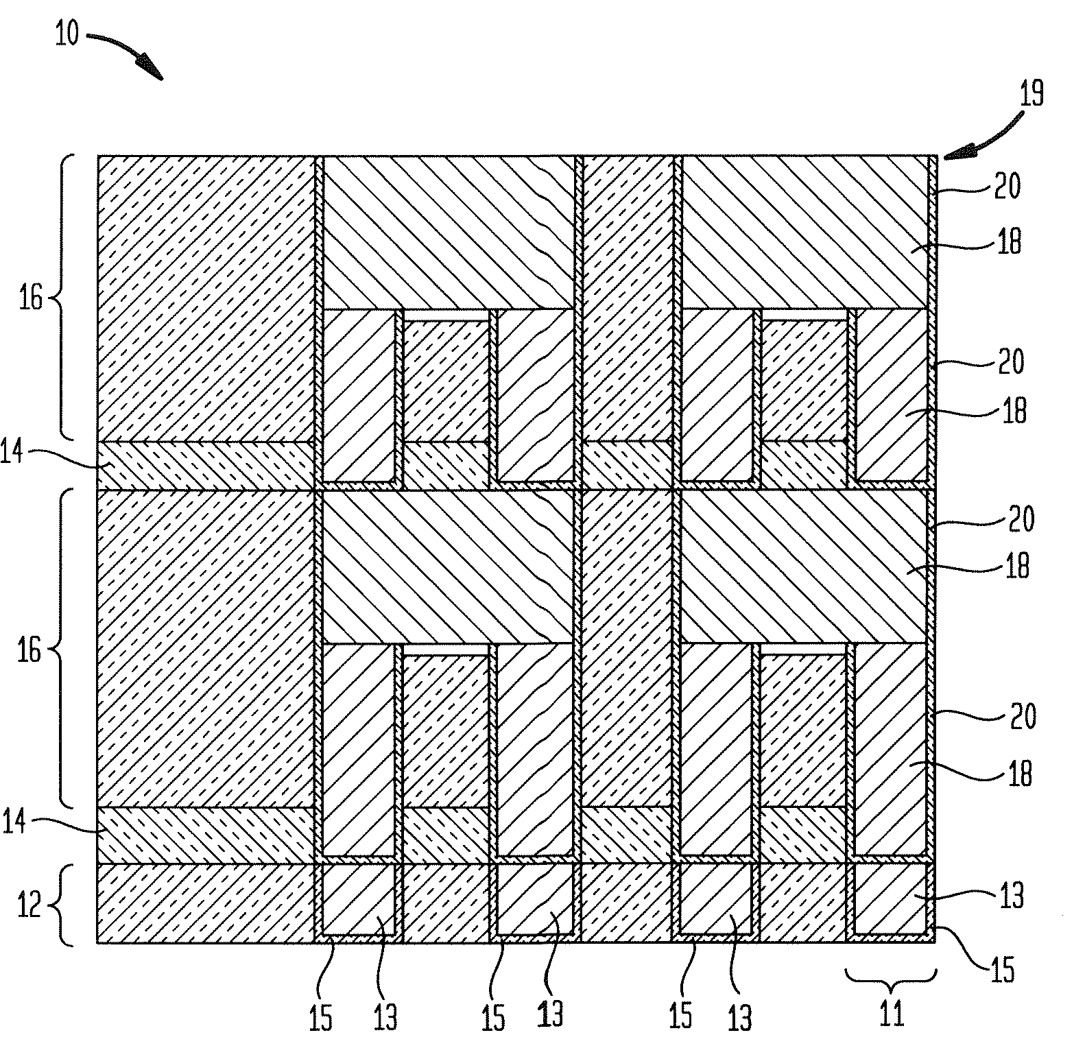
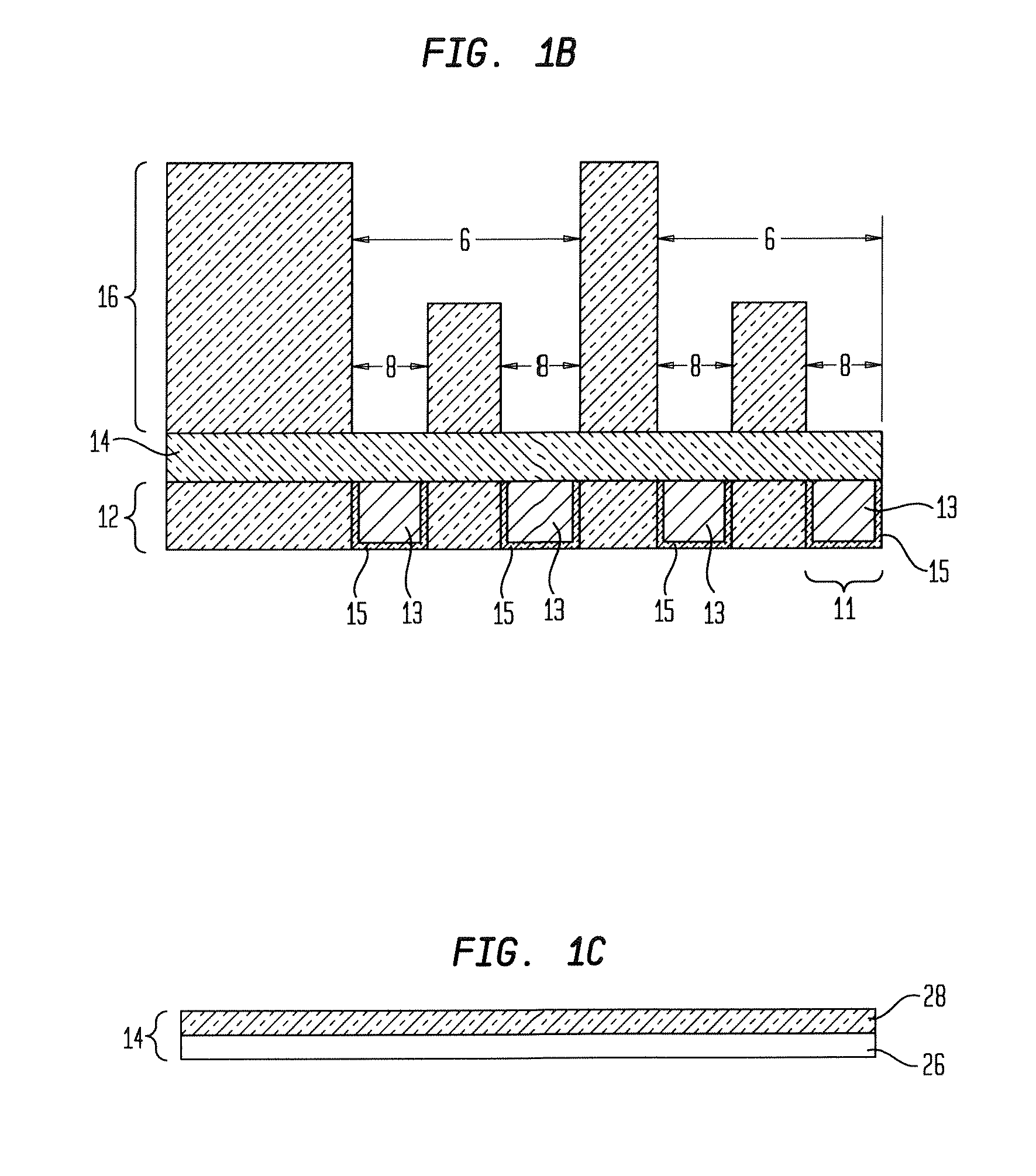
[0028]The present invention, which describes a boron-based or phosphorus-based dielectric material, a method of fabricating the same, electronic structures including the boron-based or phosphorus-based dielectric and methods of fabricating such electronic structures, will now be described in greater detail by referring to the following discussion and drawings that accompany the present application. It is noted that the drawings of the present application are provided for illustrative proposes and, as such, they are not drawn to scale.

[0029]In the following description, numerous specific details are set forth, such as particular structures, components, materials, dimensions, processing steps and techniques, in order to provide a thorough understanding of the present invention. However, it will be appreciated by one of ordinary skill in the art that the invention may be practiced without these specific details. In other instances, well-known structures or processing steps have not bee...


PUM


Abstract

A dense boron-based or phosphorus-based dielectric material is provided. Specifically, the present invention provides a dense boron-based dielectric material comprised of boron and at least one of carbon, nitrogen, and hydrogen or a dense phosphorus-based dielectric comprised of phosphorus and nitrogen. The present invention also provides electronic structures containing the dense boron-based or phosphorus-based dielectric as an etch stop, a dielectric Cu capping material, a CMP stop layer, and/or a reactive ion etching mask in a ULSI back-end-of-the-line (BEOL) interconnect structure. A method of forming the inventive boron-based or phosphorus-based dielectric as well as the electronic structure containing the same are also described in the present invention.

Description

FIELD OF THE INVENTION[0001]The present invention describes dielectric materials comprised of boron or phosphorus in combination with other elements that have high thermal and chemical stability, and methods for fabricating films of these materials and electronic devices containing such films. More particularly, the present invention relates to a dense boron alloy or dense phosphorus alloy dielectric material for use as an etch stop, a cap material, and / or a hard mask / polish stop in an ultra large scale integrated (ULSI) back-end-of-the-line (BEOL) interconnect structure. Electronic structures containing these materials are provided, and methods for fabrication of such films and structures are also described.BACKGROUND OF THE INVENTION[0002]The continuous shrinking in dimensions of electronic devices utilized in ULSI circuits in recent years has resulted in increasing the resistance of the BEOL metallization as well as increasing the capacitance of the intralayer and interlayer diel...

Claims


Application Information

Patent Timeline
IPC IPC(8): H01L23/52H01L21/469C01B35/00C01B25/00
CPCH01L21/31116H01L21/31144H01L2924/0002H01L21/31604H01L21/318H01L21/3212H01L21/76807H01L21/76829H01L21/76832H01L21/76834H01L21/76835H01L23/53238H01L23/5329H01L23/53295H01L2924/00H01L21/02205H01L21/02112
Inventor GATES, STEPHEN M.MILLER, ROBERT D.
Owner GLOBALFOUNDRIES INC
Why Eureka
Try Eureka