Programmable semiconductor device

a technology of programmable semiconductors and semiconductors, applied in semiconductor/solid-state device testing/measurement, semiconductor/solid-state device details, instruments, etc., can solve the problems of fuse pitch, post-collateral damage of neighboring structures, and known semiconductor e-fuses that have not been completely satisfactory

Inactive Publication Date: 2007-12-27
GLOBALFOUNDRIES INC
View PDF19 Cites 10 Cited by
  • Summary
  • Abstract
  • Description
  • Claims
  • Application Information

AI Technical Summary

Benefits of technology

[0005] The present invention overcomes this and other drawbacks by employing a device or fuse structure of a composite material that migrates during a programming event. The material that migrates (e.g., WSi2) changes state, and does not cause collateral damage during its migration or material reformation, and has a programmed state where ±ΔRp is preferably equal to zero. This allows for individual fuses to discriminate among themselves and to eliminate unwanted reference fuse elements, as well as the circuitry used to bias and compare against the reference fuse elements.
[0009] It is a principal object of the present invention to provide a programmable semiconductor device which does not cause collateral damage to adjacent devices or other elements during programming.
[0010] It is a further object of the present invention to provide a method of fabricating a programmable semiconductor device, which method is readily compatible with various standard MOS manufacturing processes.
[0011] It is an additional object of the present invention to provide a method of programming a programmable semiconductor device which reduces collateral damages to neighboring structures.

Problems solved by technology

However, known semiconductor E-fuses have not proven to be entirely satisfactory.
Programming in silicon-based semiconductor devices (e.g., fuses) can result in post collateral damage of the neighboring structures.
This result typically forces a fuse pitch, or fuse cavity, set of rules that do not scale well with the technology feature rules from one generation to the next.
Thus, fuse density and effectiveness of fuse repair, replacement, or customization are limited.
Typically, such damage is caused by particulates from fuse blow.
It is the ±ΔRp that causes fuse read instability because this parameter is statistical in nature.
The variations that cause the R0 and Rp distributions to approach each other cause practical limitations in interrogating a programmed fuse through a standard CMOS latching circuit.
Such practices result in unwanted growth in the fuse bank area.

Method used


Image

  • Programmable semiconductor device
  • Programmable semiconductor device
  • Programmable semiconductor device

Examples


Embodiment Construction

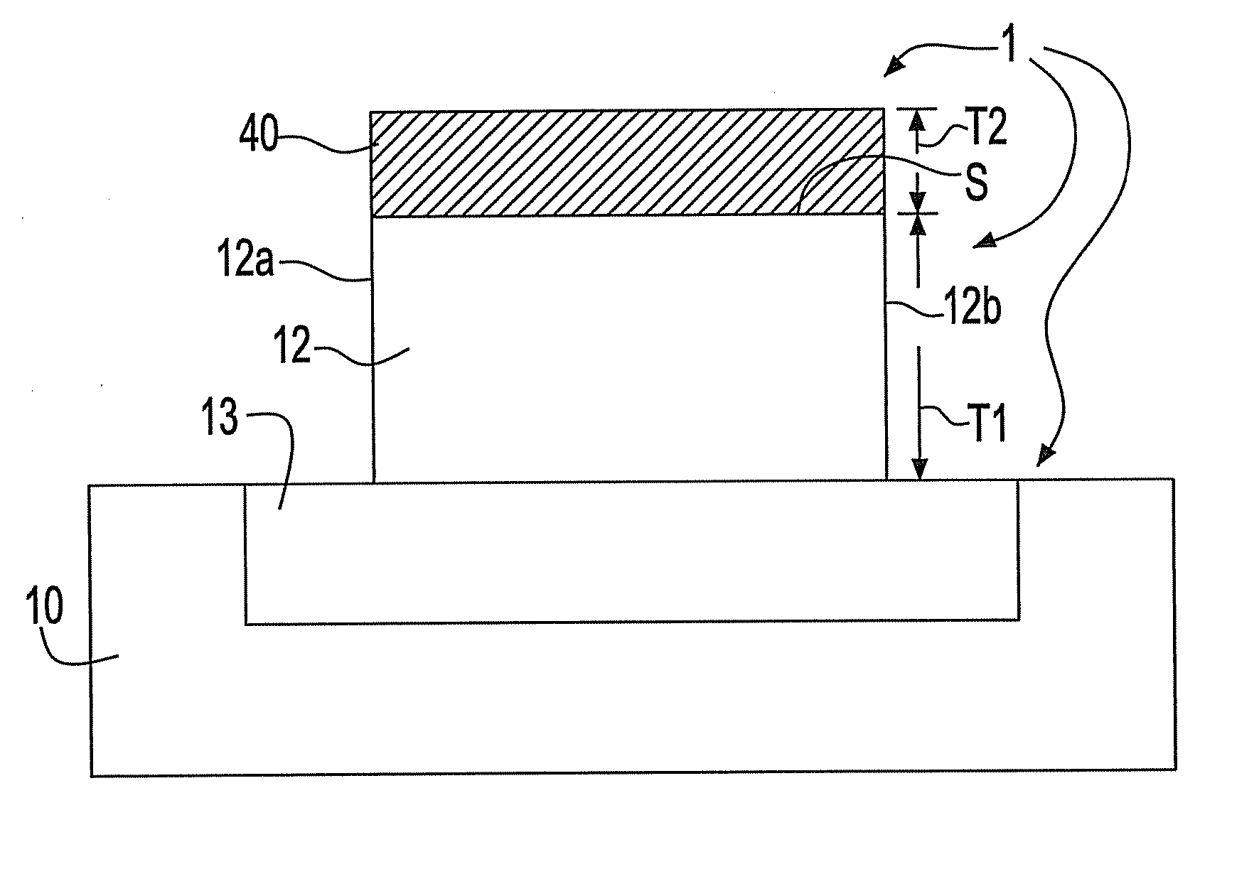
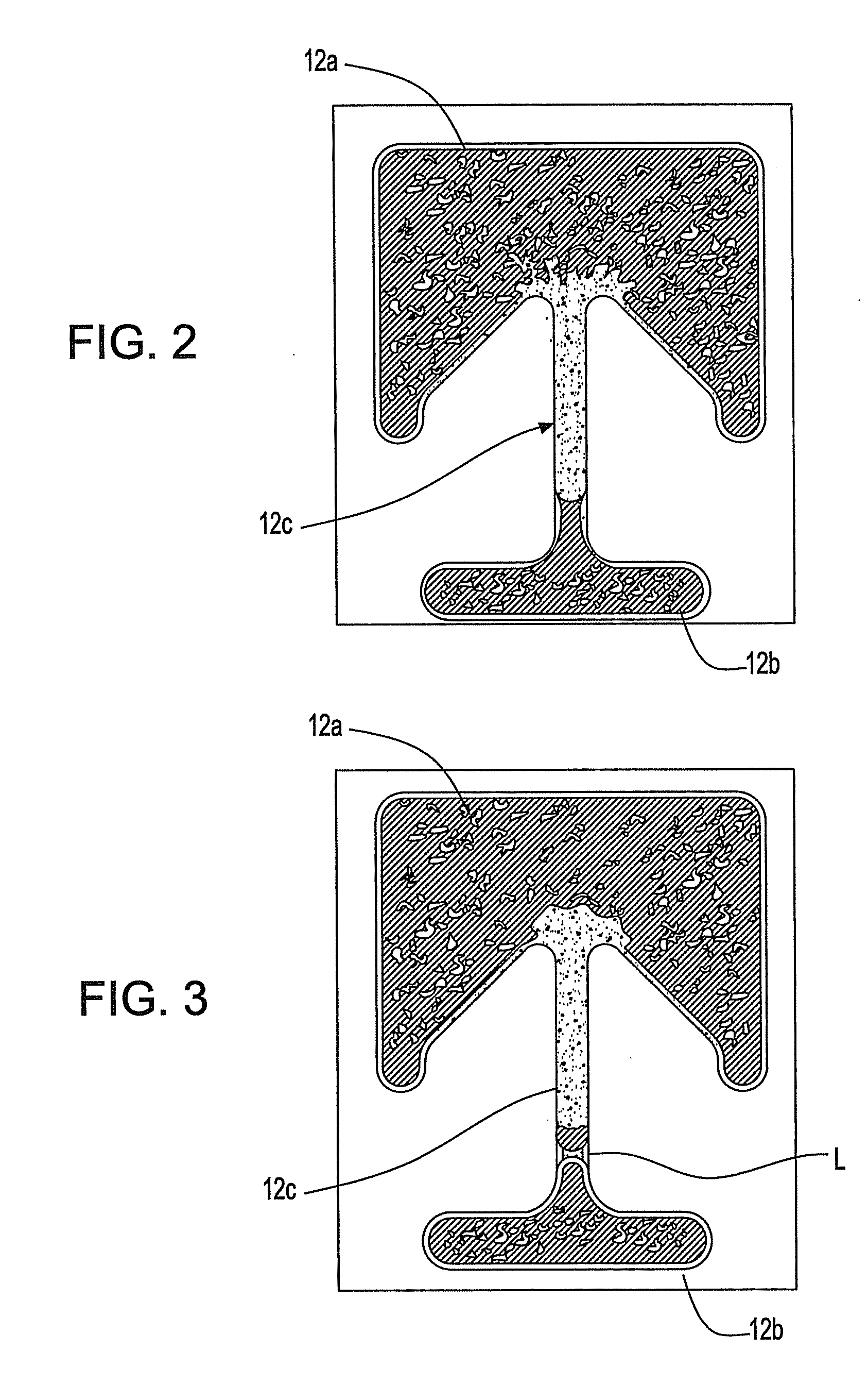
[0022]FIG. 1 shows a preferred programmable (un-programmed) semiconductor device (1) (e.g. fuse) in cross section. The fuse (1) includes an elongated semiconductor material (12) having a metallic material (40) disposed on an upper surface S. The material (12) is disposed on / over an isolation region (13) in a silicon substrate (10). Preferably, the unprogrammed fuse includes N+ polysilicon (90 nm height / thickness T1) (12) and WSi2 (55 nm height / thickness T2) (40). The region (13) is, for example, filled with an insulator such as an oxide. The region (13) is, for example, a known shallow trench isolation (STI) region. The device (1) includes a first end (12a), a second end (12b) and a central portion or link (12c) connecting the first end (12a) to the second end (12b). Preferably, the link (12c) and the second end (12b), together, form a “T”-shaped member (FIG. 2, and FIGS. 11a, 11b).

[0023] According to an important feature of the present invention, the resistivity of the metallic ma...


PUM


Abstract

A design structure for designing and manufacturing a programmable device. The design structure includes a substrate (10); an insulator (13) on the substrate; an elongated semiconductor material (12) on the insulator, the elongated semiconductor material having first and second ends, and an upper surface S; the first end (12a) is substantially wider than the second end (12b), and a metallic material is disposed on the upper surface; the metallic material being physically migratable along the upper surface responsive to an electrical current I flowable through the semiconductor material and the metallic material.

Description

CROSS REFERENCE TO RELATED APPLICATION [0001] This application is a continuation in part of pending U.S. application Ser. No. 10 / 552,971 filed Oct. 11, 2005, which is a continuation of PCT application serial no. PCT / U503 / 13392 filed 30 Apr. 2003, which claims priority of provisional application Ser. No. 60 / 462,568, filed 11 Apr. 2003; all assigned to the present assignee.TECHNICAL FIELD [0002] The present invention relates to programmable semiconductor devices and, more particularly, to design structures which comprise such devices usable as semiconductor electronic (E) fuses. BACKGROUND [0003] Semiconductor E-fuses in general are known. See, for example, U.S. Pat. No. 5,334,880, Low Voltage Programmable Storage Element, issued Aug. 2, 1994, by Abadeer et al., which is incorporated herein in its entirety. [0004] However, known semiconductor E-fuses have not proven to be entirely satisfactory. Programming in silicon-based semiconductor devices (e.g., fuses) can result in post collate...

Claims


Application Information

Patent Timeline
Patent Type & Authority Applications(United States)
IPC IPC(8): G01R31/26H01L23/525
CPCG11C17/16H01L23/5256H01L2924/0002H01L2924/00H01L29/04
Inventor BERRY, WAYNE S.FIFIELD, JOHN ATKINSONGUTHRIE, WILLIAM H.KONTRA, RICHARD STEVENTONTI, WILLIAM ROBERT
Owner GLOBALFOUNDRIES INC
Why Eureka
Try Eureka