Vertical Field-Effect Transistor and Method of Forming the Same

a technology of vertical field effect transistor and transistor, which is applied in the direction of semiconductor devices, basic electric elements, electrical appliances, etc., can solve the problems of limited marketability in view of the presently available silicon-based technology, limiting the applicability of the device in certain situations, and limiting the switching speed and operation as an enhancement-mode devi

Active Publication Date: 2007-12-27
MYPAQ HLDG LTD
View PDF40 Cites 61 Cited by
  • Summary
  • Abstract
  • Description
  • Claims
  • Application Information

AI Technical Summary

Benefits of technology

[0017]These and other problems are generally solved or circumvented, and technical advantages are generally achieved, by advantageous embodiments of the present invention, which includes a semiconductor device, a method of forming the same, and a power converter including the semiconductor device. In one embodiment, the semiconductor device includes a heavily doped substrate, a source / drain contact below the heavily doped substrate, and a channel layer above the heavily doped substrate. The semiconductor device also includes a heavily doped source / drain layer above the channel layer and another source / drain contact above the heavily doped source / drain layer. The semiconductor device further includes pillar regions through the another source / drain contact, the heavily doped source / drain layer, and portions of the channel layer to form a vertical cell therebetween. Non-conductive regions of the semiconductor device are located in the portions of the channel layer within the pillar regions. The semiconductor device still further includes a gate above the non-conductive regions in the pillar regions.

Problems solved by technology

The structure as generally described in the aforementioned references has higher channel and gate resistance per unit die area than the desired resistance and produces a device operable only in the depletion mode, which may limit the applicability of the device in certain situations.
The resulting cost and performance, particularly the manufacturing cost to grow the necessary device structures in regions around and including buried gates, have resulted in limited marketability in view of the presently available silicon-based technology.
Although economies of manufacture are achieved using implants rather than etching and epitaxial growth as described by Eisenbeiser, et al., possible disadvantages of a channel so formed adjacent to a buried semiconductor gate structure limit the switching speed and operation as an enhancement-mode device.
Designing the source and drain contacts on the same surface of the die requires a complicated multilayer metallization process and results in increased die area and reduced chip yield.
Although this arrangement can provide low-inductance external connections to the source, it is limited in its ability to provide a low-resistance channel tightly coupled to the lower surface of a highly conductive substrate.
The aforementioned design also does not accommodate large drain contacts desirable for a higher power device, which will increase the resistive and inductive losses.
This configuration requires a complex air-bridge processing step, which will increase the cost and potentially affect the reliability of the device.
This design also is incompatible with today's packaging techniques for higher power devices embodied in a vertical device configuration.
The aforementioned devices, however, are formed with contacts on a top surface, which restricts their application from low voltage, high current systems wherein efficiency is an important design element.
Corresponding limitations are found in power supplies designed with power switches formed of compound semiconductor devices.
Power supply design limitations resulting from the limited performance available from power switches limit power supply switching frequency, efficiency, and power conversion density, particularly in applications powering low-voltage loads that draw high currents.
Considering the limitations as described above, a field-effect transistor design is not presently available for the more severe applications that lie ahead.

Method used


Image

  • Vertical Field-Effect Transistor and Method of Forming the Same
  • Vertical Field-Effect Transistor and Method of Forming the Same
  • Vertical Field-Effect Transistor and Method of Forming the Same

Examples


Embodiment Construction

[0025]The making and using of the presently preferred embodiments are discussed in detail below. It should be appreciated, however, that the present invention provides many applicable inventive concepts that can be embodied in a wide variety of specific contexts. The specific embodiments discussed are merely illustrative of specific ways to make and use the invention, and do not limit the scope of the invention.

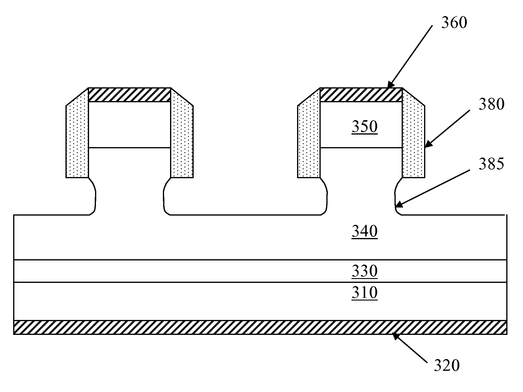
[0026]The present invention will be described first with respect to exemplary embodiments in a specific context, namely, a semiconductor device and, more particularly, a semiconductor device including a vertical FET. A vertical FET is formed with a source contact formed on a substrate (e.g., a source) and a drain contact formed on an opposing surface of the semiconductor device to provide a low on-resistance switch with very fast switching transition times. A metallized gate controls a vertical channel therein. Alternatively, the positions of the source and drain may be rever...


PUM


Abstract

A semiconductor device, a method of forming the same, and a power converter including the semiconductor device. In one embodiment, the semiconductor device includes a heavily doped substrate, a source/drain contact below the heavily doped substrate, and a channel layer above the heavily doped substrate. The semiconductor device also includes a heavily doped source/drain layer above the channel layer and another source/drain contact above the heavily doped source/drain layer. The semiconductor device further includes pillar regions through the another source/drain contact, the heavily doped source/drain layer, and portions of the channel layer to form a vertical cell therebetween. Non-conductive regions of the semiconductor device are located in the portions of the channel layer within the pillar regions. The semiconductor device still further includes a gate above the non-conductive regions in the pillar regions. The semiconductor device may also include a Schottky diode including the channel layer and a Schottky contact.

Description

[0001]This application claims the benefit of U.S. Provisional Application No. 60 / 815,479, entitled “Vertical Field-Effect Transistor and Method of Forming the Same,” filed on Jun. 21, 2006, which is incorporated herein by reference.TECHNICAL FIELD[0002]The present invention is directed, in general, to a compound semiconductor device and, more specifically, to a compound semiconductor device including a vertical field-effect transistor, a method of forming the same, and a power supply including a compound semiconductor device including a vertical field-effect transistor.BACKGROUND[0003]A field-effect transistor (also referred to as a “FET”) is a conventional semiconductor device employable in switch-mode power supplies (also referred to as “power converters”) for use in data processing and telecommunication systems as well as for other applications that use conditioned power for the operation of sensitive electronic circuits. Field-effect transistors have almost universally replaced ...

Claims


Application Information

Patent Timeline
Patent Type & Authority Applications(United States)
IPC IPC(8): H01L21/8234
CPCH01L21/823487H01L29/872H01L29/8122H01L29/66848
Inventor BRAR, BERINDER P. S.HA, WONILL
Owner MYPAQ HLDG LTD
Why Eureka
Try Eureka