Method of eliminating surface stress of silicon wafer

a technology of surface stress and silicon wafer, which is applied in the field of eliminating can solve the problems of increasing the cost of production, and increasing the leakage current. , to achieve the effect of reducing or eliminating the surface stress of silicon wafer, low cost and effective elimination

Inactive Publication Date: 2007-12-27
LIU YULING +5
View PDF15 Cites 6 Cited by
  • Summary
  • Abstract
  • Description
  • Claims
  • Application Information

AI Technical Summary

Benefits of technology

[0009]In one aspect of the invention provided is a method for overcoming the shortcomings of the conventional remnant stress removal techniques. The method comprises decentralizing and decomposing the remnant stress and preventing the surface stress centralized area from expanding in order to eliminate the surface stress of the silicon wafer.
[0016]In certain embodiments, the anti-stress groove(s) can reduce or eliminate the surface stress of silicon wafer effectively to avoid a slip line and dislocation arrangement, which may induce the p-n junctions to conduct or to increase the leakage current. The formation of anti-stress groove(s) is of low cost and is a highly efficient process. It is simple to operate and there is no need to replace or substitute the existing silicon processing equipments.

Problems solved by technology

Because silicon undergoes strong mechanical deformations during the molding process, the edge area of a wafer can be damaged as stress centralizes therein and produces cracks and micro splits.
However, mechanical action of polishing may lead to new damage and migration of stress to deeper levels of the wafer, which may be even more difficult to eliminate.

Method used


Image

  • Method of eliminating surface stress of silicon wafer
  • Method of eliminating surface stress of silicon wafer

Examples


example 1

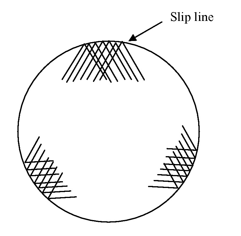
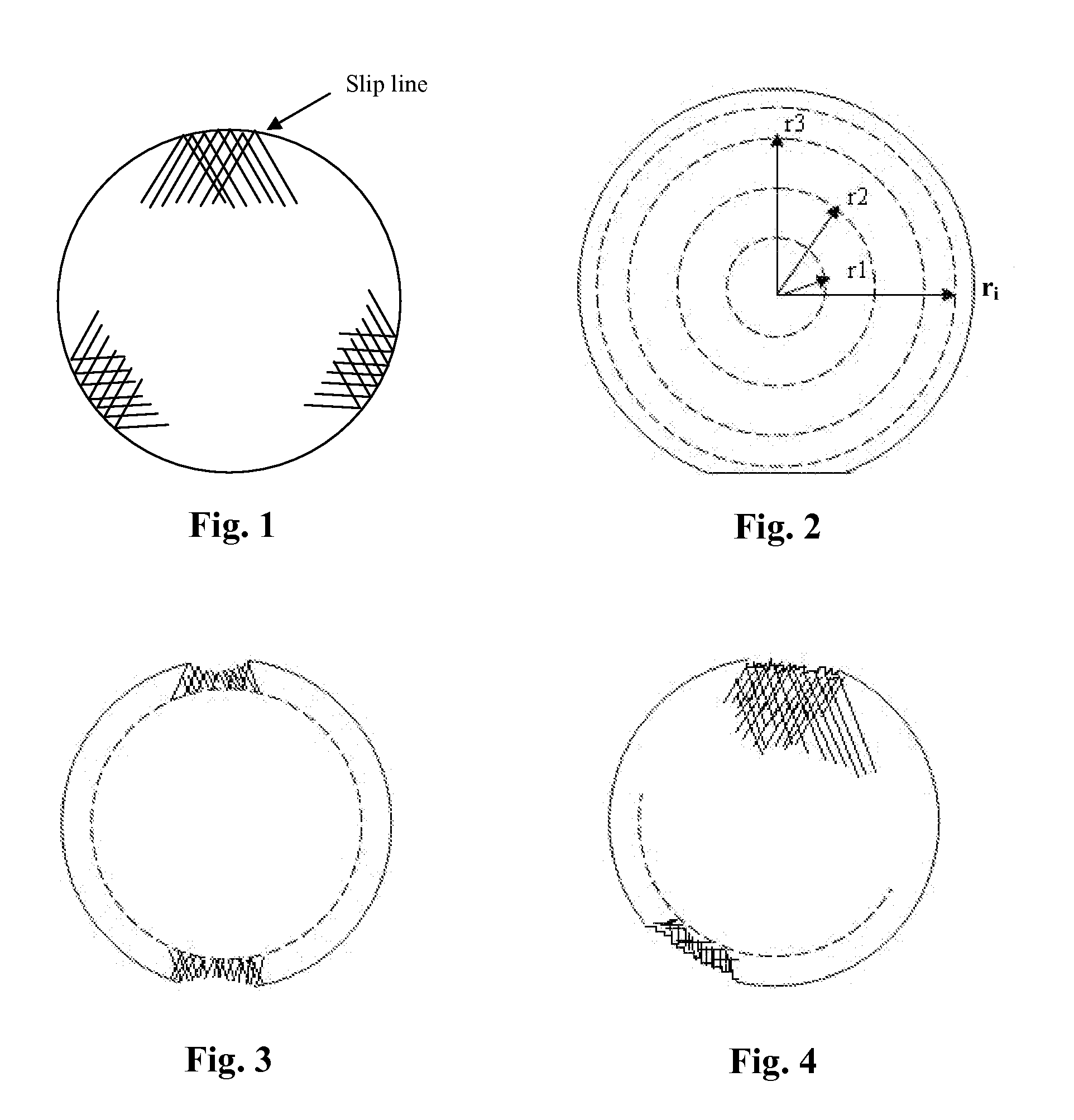
The Effect of a Closed Anti-Stress Groove on the Formation of Slip Lines

[0025]A silicon wafer with radius φ=35 mm and resistivity of 2-3×10³Ω·cm was used in the experiment. The wafer was grinded and epitaxial growth was completed at 1200° C. Thereafter, a closed anti-stress groove was scored with a diamond blade at 3 mm from the edge of wafer. No slip lines were observed.

example 2

The Effect of two Closed Anti-Stress Grooves on the Formation of Slip Lines

[0026]Two uniform wafers, A and B, with radius φ=50 mm and resistivity 2-3×10³Ω·cm were studied. Wafer A was scored with one groove at 3 mm from the edge of wafer, while wafer B was scored with two grooves: one at 3 mm from the edge of the wafer and the other at 12.5 mm from the center of the wafer. Thereafter, the wafers were grinded and epitaxial growth was completed at 1200° C. On wafer A, no slip lines were observed within 20 mm from edge, but there was a shallow slip line close to the wafer centre. On wafer B, no slip lines were observed.

example 3

The Effect of Several Closed Anti-Stress Grooves on the Formation of Slip Lines

[0027]Two uniform wafers, A and B, with radius φ=100 mm and resistivity 2-3×10³Ω·cm were studied. Wafer A was scored with two grooves: one at 3 mm from the edge of wafer and the other at 37.5 mm from the center. Wafer B was scored with four grooves: one at 3 mm from the edge of wafer, and the other ones at 2.5 mm, 25 mm and 37.5 mm from the center, respectively. Thereafter, the wafers were grinded and epitaxial growth was completed at 1200° C. On wafer A, no slip lines were observed within 60 mm from edge, but there was a shallow slip line close to the wafer centre. On wafer B, no slip lines were observed.


PUM

PropertyMeasurementUnit
angleaaaaaaaaaa
surface stressaaaaaaaaaa
thicknessaaaaaaaaaa

Abstract

This invention provides a method for eliminating the surface stress of a silicon wafer comprising forming one or more anti-stress groove(s) on the surface of the silicon wafer. These anti-stress grooves can reduce or eliminate the surface stress of silicon wafer effectively to avoid the formation of slip lines and dislocation arrangements, which may induce the p-n junction to conduct or the leakage current to increase. The process is highly efficient and low in cost. It is simple to manage and does not require additional equipment beyond that already used for processing of silicon wafers.

Description

CROSS-REFERENCE TO RELATED APPLICATIONS[0001]Pursuant to 35 U.S.C. §119 and the Paris Convention Treaty, this application claims the benefit of Chinese Patent Application No. 200610014440.8 filed Jun. 23, 2006, the contents of which are incorporated herein by reference.BACKGROUND OF THE INVENTION[0002]1. Technical field[0003]This invention relates to semiconductor technology, and especially to a method of eliminating surface stress of a silicon wafer.[0004]2. Background of the Invention[0005]Research indicates that about 98% of the remnant stress of a silicon wafer as substrate for ultra large-scale integrated circuits (ULSI) arises during mechanical processing of silicon wafers, incl. slicing, grinding, rounding, and chamfer.[0006]Because silicon undergoes strong mechanical deformations during the molding process, the edge area of a wafer can be damaged as stress centralizes therein and produces cracks and micro splits. The surface tension on a silicon wafer induces the stress to e...

Claims


Application Information

Patent Timeline
Patent Type & Authority Applications(United States)
IPC IPC(8): B24B1/00
CPCH01L21/3043B28D5/022
Inventor LIU, YULINGZHANG, JIANXINLI, WEIWEIHUANG, YANYANBIAN, YONGCHAOLIU, NA
Owner LIU YULING
Why Eureka
Try Eureka