Semiconductor device and manufacturing method thereof

a technology of semiconductor devices and manufacturing methods, applied in the direction of semiconductor devices, basic electric elements, electrical devices, etc., can solve the problems of less precise method of manufacturing semiconductor devices with laser direct drawing apparatus, electron beam direct drawing apparatus, etc., to prevent the heating of either source region and drain region, improve reliability, and prevent adverse effects of

Inactive Publication Date: 2008-01-03
SEMICON ENERGY LAB CO LTD
View PDF31 Cites 21 Cited by
  • Summary
  • Abstract
  • Description
  • Claims
  • Application Information

AI Technical Summary

Benefits of technology

[0047]Owing to this, heating of either one of the source region and the drain region can be prevented, thereby preventing an adverse effect on the TFT.
[0048]According to the above description, it is clear that the present invention enables the manufacturing of a TFT for forming a memory cell in a ROM with improved reliability.

Problems solved by technology

On the other hand, data identification utilizing bar codes is disadvantageous in that a bar code reader is required to be in contact with the bar codes, and that the amount of data capable of being stored in the bar codes is small.
However, the mask ROM (hereinafter simply referred to as a ROM) can only write data at the time of manufacturing.
Thus, when the individual data such as the ID numbers are formed to be all different, a heavy burden is imposed on manufacturing cost and the manufacturing process.
However, the method for manufacturing the semiconductor device with the laser direct drawing apparatus, an electron beam direct drawing apparatus, or the like is less precise than a method using photolithography.
In addition, when the laser direct drawing apparatus, the electron beam direct drawing apparatus, or the like is used, there is a possibility that a manufactured semiconductor device may not match the design rule.

Method used


Image

  • Semiconductor device and manufacturing method thereof
  • Semiconductor device and manufacturing method thereof
  • Semiconductor device and manufacturing method thereof

Examples


embodiment mode 1

[0075]Embodiment Mode 1 will be described with reference to FIGS. 1, 5, 7, 8A and 8B, 9, 10, 12A to 12D, 13A to 13C, 14A to 14C, and 15. Note, while thin film transistors having a top gate configuration are shown, they may also have a bottom gate configuration instead of the top gate configuration.

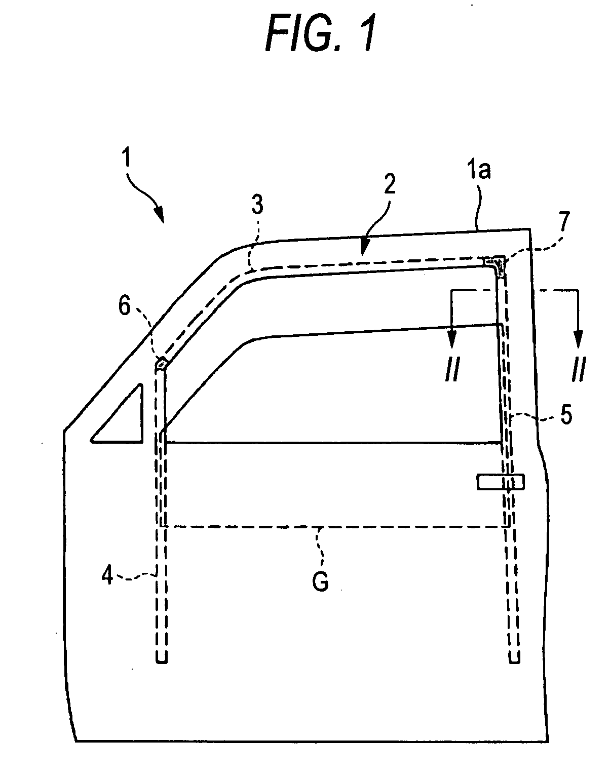
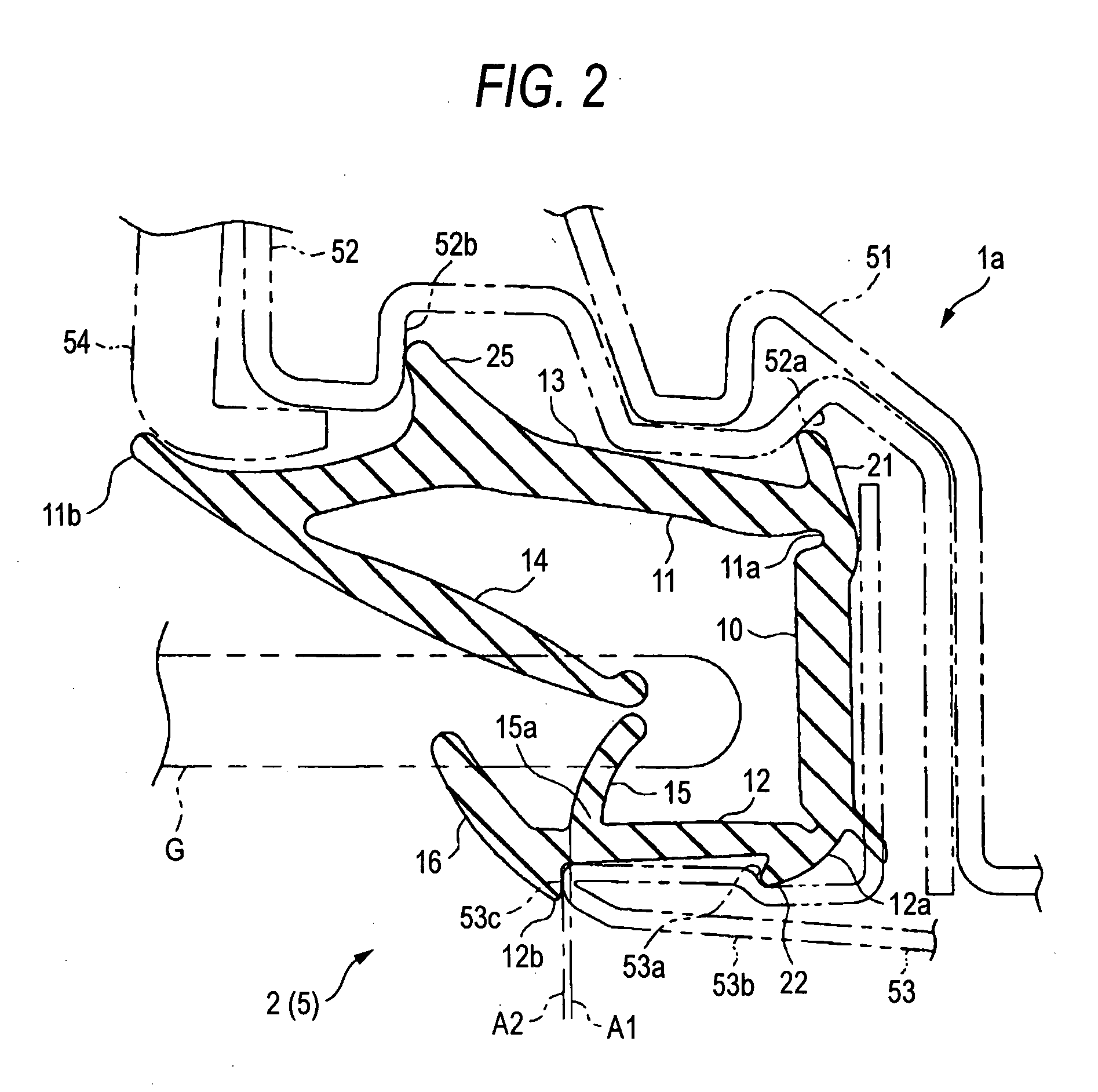
[0076]FIG. 1 is a top view of a memory cell array in a mask ROM, and FIG. 7 is a cross sectional view taken along a line A-A′ in FIG. 1.

[0077]The storage state of the mask ROM shown in FIGS. 1 and 7 is expressed by whether or not a contact hole is formed to reacha source region or a drain region of a TFT that forms a memory cell that is formed in the mask ROM.

[0078]For simplicity, FIGS. 1 and 7 show a memory cell array for 4 bits. However, a nonvolatile memory circuit of the present invention is not limited to 4 bits.

[0079]In FIGS. 1 and 7, TFTs 118 to 121 are n-channel TFTs, and the TFT 118 includes an island-like semiconductor film 131, which is an active layer, and a gate electrode 103 ...

embodiment mode 2

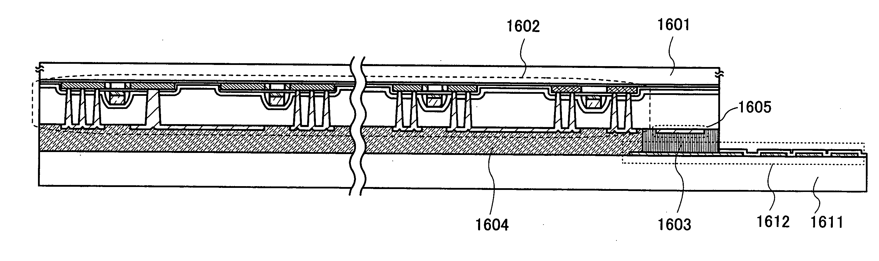
[0190]In Embodiment Mode 2, a semiconductor device capable of wireless communication with the use of an IC, which includes a mask ROM having a structure different from that of Embodiment Mode 1 will be described with reference to FIG. 16 and FIG. 17. Embodiment Mode 1 may be incorporated into a detailed manufacturing process of this embodiment mode.

[0191]FIG. 16 is a top view of this embodiment mode, and FIG. 17 is a cross sectional view taken along a line C-C′ and a line D-D′ in FIG. 16. Note, while thin film transistors having a top gate configuration are shown, they may also have a bottom gate configuration instead of the top gate configuration.

[0192]In Embodiment Mode 1, the individual data such as an ID number is determined by whether to form the contact hole 141 and the contact hole 680, which are formed with a laser direct drawing apparatus or the like. However, in this embodiment mode, contact holes formed with a laser direct drawing apparatus or the like are formed in all T...

embodiment mode 3

[0206]Embodiment Mode 3 will describe a manufacturing method of a semiconductor device capable of wireless communication with the use of an IC, which is different from those in Embodiment Modes 1 and 2 with reference to FIGS. 18A and 18B, FIGS. 19A and 19B, and FIG. 20. In this embodiment mode, components which are the same as those in Embodiment Mode 1 are denoted by the same reference numerals. Note, while thin film transistors having a top gate configuration are shown, they may also have a bottom gate configuration instead of the top gate configuration.

[0207]First, in accordance with the description in Embodiment Mode 1, a semiconductor device shown in FIG. 15 is manufactured. Note that instead of the base film 602, a separation layer 802, a first base film 803, and a second base film 804 are formed.

[0208]The separation layer 802 is formed of an amorphous semiconductor film, a polycrystalline semiconductor film, or a semi-amorphous semiconductor film. For example, a layer mainly ...


PUM


Abstract

An individual identifier is easily provided in a semiconductor device capable of wireless communication. The semiconductor device includes a thin film transistor including a channel forming region, an island-like semiconductor film including a source region and a drain region, a gate insulating film, and a gate electrode; an interlayer insulating film; a plurality of contact holes formed in the interlayer insulating film which reach one of the source region and the drain region; and a single contact hole which reaches the other of the source region and the drain region, wherein a diameter of the single contact hole is larger than a diameter of each of the plurality of contact holes, and a sum of areas of bases of the plurality of contact holes is equal to an area of a base of the single contact hole.

Description

BACKGROUND OF THE INVENTION[0001]1. Field of the Invention[0002]The present invention relates to semiconductor devices capable of communication with the use of contactless means such as wireless communication, and a manufacturing method thereof. In particular, the present invention relates to a semiconductor device that is formed over an insulating substrate of glass, plastic, or the like and a manufacturing method thereof.[0003]2. Description of the Related Art[0004]With development of computer technologies and improvement of image recognition technologies, data identification methods utilizing a medium such as bar codes have spread widely and have been used for identification of product data and the like. It is expected that the amount of data to be identified will further increase in the future. On the other hand, data identification utilizing bar codes is disadvantageous in that a bar code reader is required to be in contact with the bar codes, and that the amount of data capabl...

Claims


Application Information

Patent Timeline
Patent Type & Authority Applications(United States)
IPC IPC(8): H01L27/12H01L21/84
CPCH01L21/76816H01L27/105H01L27/112H01L27/1255H01L27/11293H01L29/41733H01L27/124H01L27/11226H10B20/34H10B20/65H10B20/00H10B99/00
Inventor SHIONOIRI, YUTAKAOHMARU, TAKURO
Owner SEMICON ENERGY LAB CO LTD
Why Eureka
Try Eureka