Method for manufacturing semiconductor device and semiconductor device
a manufacturing method and technology for semiconductor devices, applied in semiconductor devices, capacitors, instruments, etc., can solve the problem that the semiconductor chip cannot be exposed completely by single exposur
- Summary
- Abstract
- Description
- Claims
- Application Information
AI Technical Summary
Benefits of technology
Problems solved by technology
Method used
Image
Examples
first embodiment
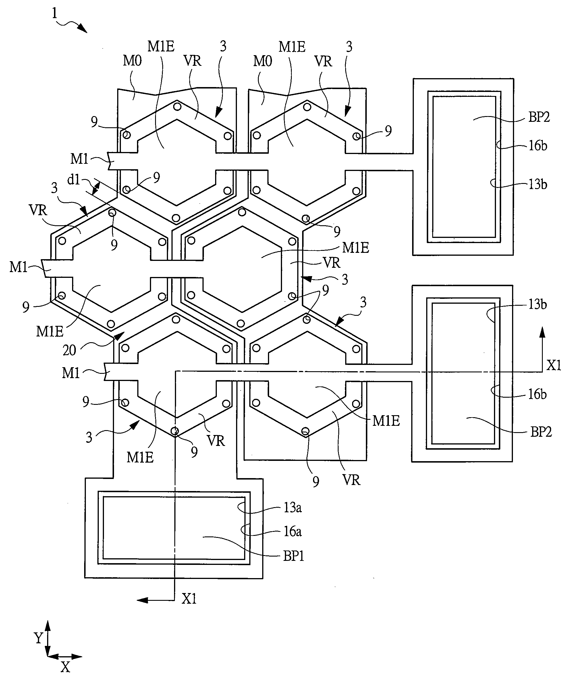
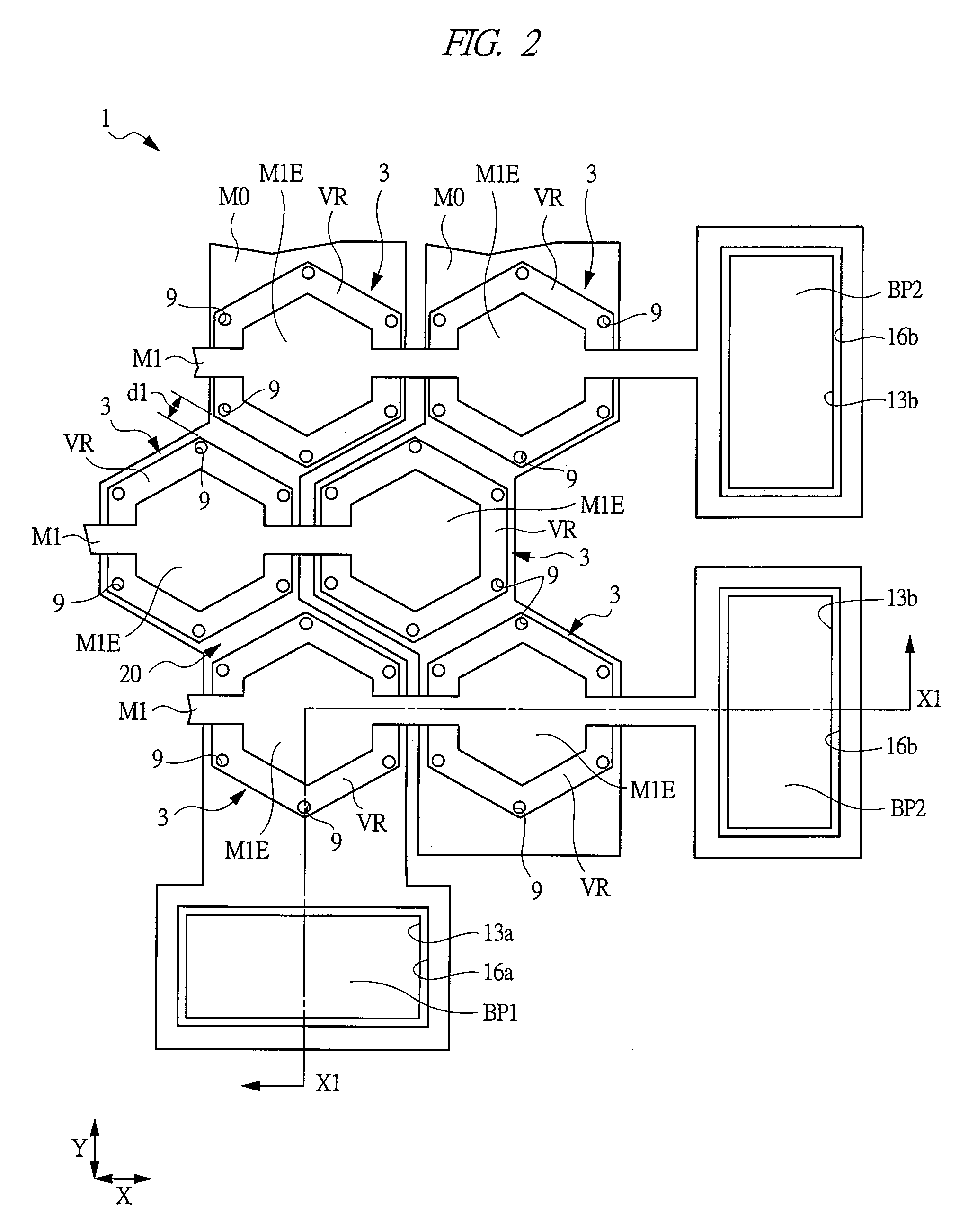
[0055]A semiconductor device according to the first embodiment is an ultrasonic transmitting / receiving sensor which is manufactured by using, for example, a MEMS (micro electro mechanical system) technology.
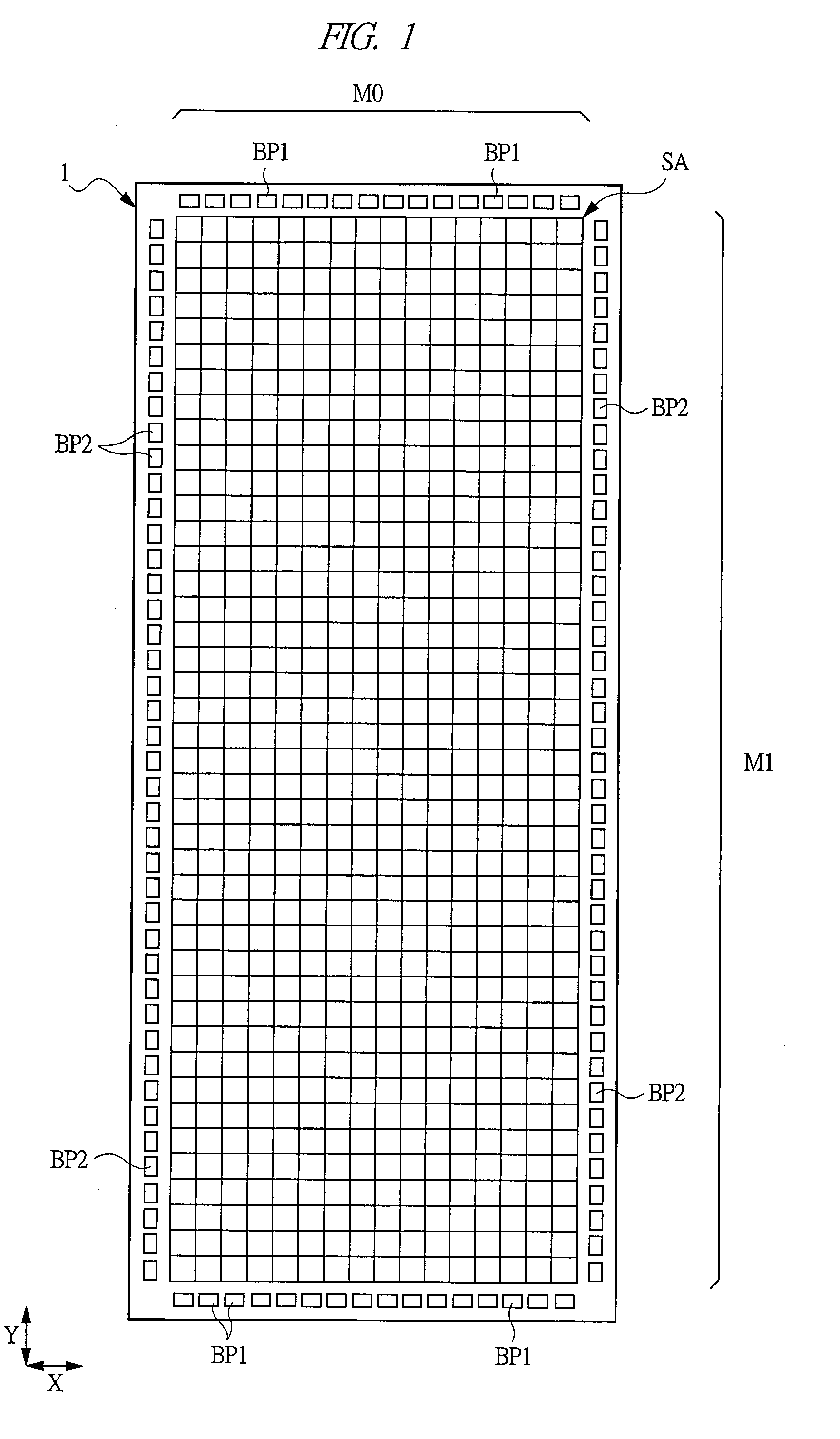
[0056]FIG. 1 is a plan view showing the entirety of a semiconductor chip 1 which constitutes the semiconductor device according to the first embodiment. The semiconductor chip 1 has a first main surface and a second main surface which are located on the opposite sides in the thickness direction. For example, the semiconductor chip 1 is formed to have a rectangular planar shape. The length of the semiconductor chip 1 in the longitudinal direction (second direction Y) is, for example, about 4 cm and the length of the semiconductor chip 1 in the short-side direction (first direction X) is, for example, about 1 cm.
[0057]However, the planar dimensions of the semiconductor chip 1 are not limited to these, and a variety of modifications are possible. There are sensors in various sizes, ...
second embodiment
[0140]FIG. 27 is an enlarged plan view illustrating the principal part of an example of the stitching exposure area SR and its peripheral areas of the semiconductor chip 1 according to a second embodiment. FIG. 28 is a sectional view taken along the line Y3-Y3 of FIG. 27. In FIG. 27, in order to make the configuration in the drawing easy to understand, the illustration of the lower electrode wirings M0 and the lower electrodes M0E is omitted.
[0141]Also in the second embodiment, the stitching exposure area SR (protrusion 15a) is arranged so as to avoid the oscillators 3 (cavity portions VR) as much as possible. More specifically, also in the second embodiment, the stitching exposure area SR is arranged so that the center CL (apex of the protrusion 15a) of the width (dimension in the short-side direction) of the stitching exposure area is positioned at the center of the line which connects the centers C0 of the adjacent oscillators 3 positioned above and below (second direction Y) the...
PUM
 Abstract
Description
Claims
Application Information


