Regulator circuit

Active Publication Date: 2008-01-03
MONTEREY RES LLC
View PDF12 Cites 39 Cited by
  • Summary
  • Abstract
  • Description
  • Claims
  • Application Information

AI Technical Summary

Benefits of technology

[0087]All the configurations as described above improve accuracy of generating a signal. Therefore, it is also possible to accomplish a generation of an (internal) power supply voltage firmly in high accuracy in addition to stability and a high speed response.
[0088]In the case of operating an amplification-use transistor comprised by the above described amplifier circuit in a saturation region, a practically adequate gain is obtained. Because of thi

Problems solved by technology

This has caused a difficulty in maintaining a balance between a stability of the loop and a response characteristic for keeping track of potentials of the signals AMPO1 and PPG1 in high speed in response to a voltage fluctuation of the internal power supply voltage VDD.
However, there is a limit in a balanced obtainment of a high speed response and stability because the second conventional example also includes a capacitor COUT for stabilizing the internal power supply voltage VDD in the feedback loop.
That is, the reference voltage Vref contains an error caused by a circuit part for generating the reference voltage Vref from the bandgap voltage Vbgr, and the error consequently degrades voltage accuracy of an internal power supply voltage VDD.
That is, a combination of the conventional circuit shown in FIG. 3 with a bandgap circuit such as the one shown in FIG. 4 is faced with a problem of an error caused by the operational amplifier circuit AMP4 shown in FIG. 4 being added to the ref

Method used


Image

  • Regulator circuit
  • Regulator circuit
  • Regulator circuit

Examples


second embodiment

[0180]The circuit shown by FIG. 7 has exemplified a circuit in the case of using each one of a replica amplifier (i.e., AMPLD2R) and a load driving amplifier (i.e., AMPLD2). Although the simplest circuit configuration has been shown for describing a fundamental operation, the circuit shown by FIG. 7 is faced with the case of an excessive increase of the potential of the internal power supply VDD occasionally at the time of turning the power on. In such a case, it is possible to prevent a potential of the internal power supply VDD from increasing excessively at the time of turning the power by configuring a circuit as shown by FIG. 15. The next is a description of a difference of the operation at the time of turning on the power between the circuit shown by FIG. 15 and the one shown by FIG. 7.

[0181]FIG. 15 shows a configuration of a regulator circuit according to the second embodiment. In the showing of FIG. 15, the same component sign is attached to the same component or fundamental...

third embodiment

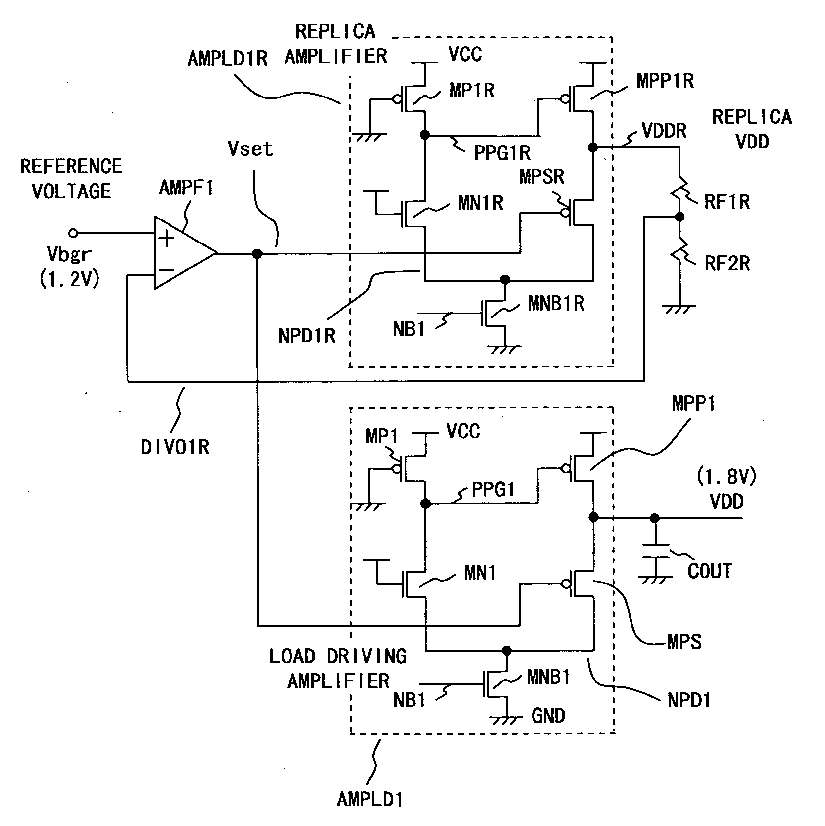
[0229]The above described first and second embodiments are configured to constitute a feedback circuit by using the operational amplifier circuit AMPF1. Such a circuit configuration provides a benefit of obtaining a large enough gain of the feedback circuit constituted by the operational amplifier circuit AMPF1 and replica amplifier even when operating the PMOS transistor MPP1 in a linear region (i.e., a voltage between the gate and source of the transistor is amply higher than the one between the drain and source thereof). The reason is that a gain of the entirety of the feedback circuit is the product of a gain of the PMOS transistor MPP1 and that of the replica amplifier, although the gain of the transistor MPP1 drastically reduces in the linear region. This makes it possible to generate a power supply voltage VDD in high accuracy even if the potential difference between the power supply voltages VCC and VDD is small.

[0230]Comparably, in the case of not operating the transistor M...


PUM


Abstract

The present invention is contrived to adopt a differential pair type amplifier circuit comprising a differential pair constituted by a first transistor receiving an input of a first signal and by a second transistor receiving an input of a third signal generated by outputting a second signal of which the voltage level is a power supply voltage. Elements requiring a matching are two transistors constituting the differential pair for the amplifier circuit. Because of this, the elements requiring a matching can be placed close to each other regardless of a layout between the amplifier circuits.

Description

CROSS REFERENCE TO RELATED APPLICATIONS[0001]This application is based upon and claims the benefit of priority from the prior Japanese Patent Application No. 2006-170741 filed on Jun. 20, 2006, the entire contents of which are incorporated herein by reference.BACKGROUND OF THE INVENTION[0002]1. Field of the Invention[0003]The present invention relates to a regulator circuit capable of responding to a variation of a load current.[0004]2. Description of the Related Art[0005]An integrated circuit, such as a micro controller unit (MCU), equipped onto a semiconductor chip is sometimes configured such that a regulator circuit is also equipped onto the semiconductor chip and the regulator circuit supplies the integrated circuit with a voltage lower than an external power supply which is externally applied. The reasons include an inability of applying a high voltage to a digital circuit (i.e., an internal power supply voltage must be reduced) because a withstand voltage of elements constitu...

Claims


Application Information

Patent Timeline
IPC IPC(8): H03F3/45
CPCH03F3/347H03F3/45183H03F3/45475H03F2203/45466H03F2200/456H03F2203/45138H03F2200/453
Inventor TACHIBANA, SUGURUARUGA, KENTAKATO, TATSUO
Owner MONTEREY RES LLC
Why Eureka
Try Eureka