Fine pitch microcontacts and method for forming thereof

a microcontact and fine pitch technology, applied in the field of microelectronic packages, can solve the problems of difficult or impossible to form microcontact arrays with appreciable height and very small pitch or spacing, and the configuration of microcontacts formed by conventional etching processes is limited

Active Publication Date: 2008-01-03
TESSERA INC
View PDF99 Cites 66 Cited by
  • Summary
  • Abstract
  • Description
  • Claims
  • Application Information

AI Technical Summary

Benefits of technology

[0010] In another embodiment, a microelectronic unit includes (a) a substrate, and (b) a plurality of microcontacts projecting in a vertical direction from the substrate, each microcontact having a proximal portion adjacent the subst

Problems solved by technology

It has been difficult or impossible to form arrays of microcontacts with appreciable height and very small pitch or spacing betwe

Method used


Image

  • Fine pitch microcontacts and method for forming thereof
  • Fine pitch microcontacts and method for forming thereof
  • Fine pitch microcontacts and method for forming thereof

Examples


Embodiment Construction

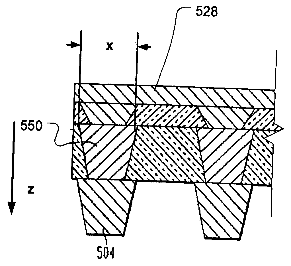
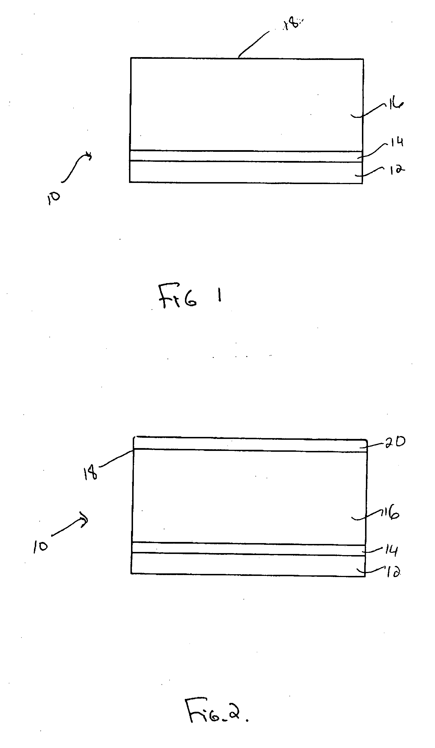
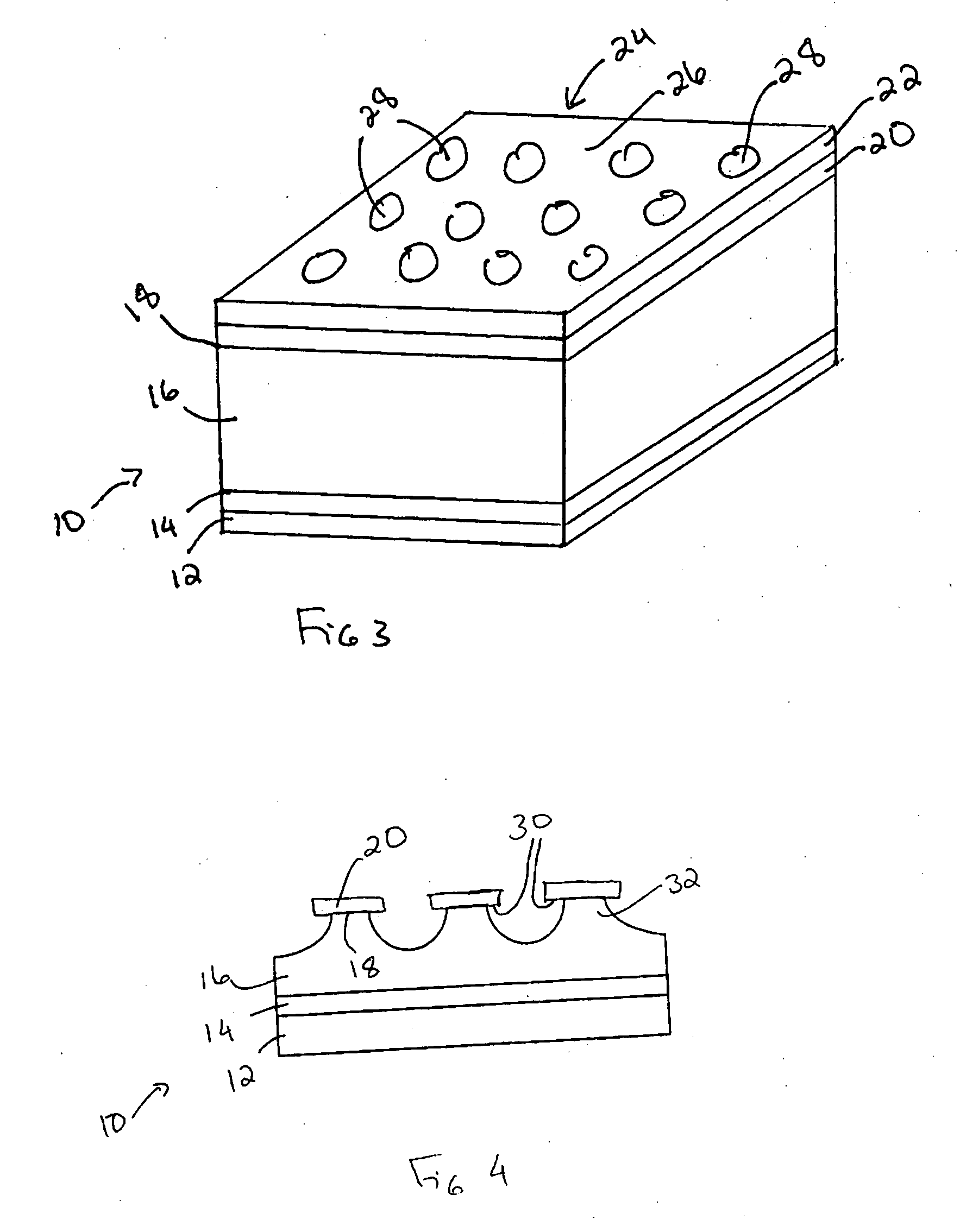
[0026] A first method or embodiment is described. FIG. 1 is a schematic illustration of a tri-metal substrate 10. The tri-metal substrate 10 has a trace layer 12, an etch stop layer 14, a thick layer 16, and a top surface 18. The trace layer 12 and the thick layer 16 may be formed of a readily etchable first metal such as copper, while the etch stop layer 14 may be formed of a metal, such as nickel, which is substantially resistant to etching by a process used to etch copper. Although, copper and nickel are recited, the substrate 10 may be formed of any suitable material as desired.

[0027]FIG. 2 is a schematic illustration of the tri-metal substrate 10 of FIG. 1 with a layer of a first photoresist 20. The first photoresist 20 is deposited onto the top surface 18. The first photoresist 20 may be any type of material that hardens or undergoes a chemical reaction when exposed to radiation such as light. Thus, any etch-resistant material maybe used. Positive and negative photoresists ma...


PUM

PropertyMeasurementUnit
Lengthaaaaaaaaaa
Diameteraaaaaaaaaa
Diameteraaaaaaaaaa

Abstract

A method includes applying a final etch-resistant material to an in-process substrate so that the final etch-resistant material at least partially covers first microcontact portions integral with the substrate and projecting upwardly from a surface of the substrate, and etching the surface of the substrate so as to leave second microcontact portions below the first microcontact portions and integral therewith, the final etch-resistant material at least partially protecting the first microcontact portions from etching during the further etching step. A microelectronic unit includes a substrate, and a plurality of microcontacts projecting in a vertical direction from the substrate, each microcontact including a base region adjacent the substrate and a tip region remote from the substrate, each microcontact having a horizontal dimension which is a first function of vertical location in the base region and which is a second function of vertical location in the tip region.

Description

CROSS-REFERENCE TO RELATED APPLICATIONS [0001] This application is a continuation-in-part of U.S. patent application Ser. No. 11 / 166,982, filed Jun. 24, 2005, which application claims the benefit of the filing date of U.S. Provisional Patent Application No. 60 / 583,109, filed Jun. 25, 2004. application Ser. No. 11 / 166,982 is also a continuation-in-part of U.S. patent application Ser. No. 10 / 959,465, filed Oct. 6, 2004. application Ser. No. 10 / 959,465 also claims the benefit of the filing dates of U.S. Provisional Patent Application No. 60 / 508,970, filed Oct. 6, 2003; 60 / 533,210, filed Dec. 30, 2003; 60 / 533,393, filed Dec. 30, 2003; and 60 / 533,437, filed Dec. 30, 2003. The disclosures of all of the aforementioned applications are hereby incorporated by reference herein.BACKGROUND OF THE INVENTION [0002] The present invention relates to microelectronic packages, to components for use in fabrication of microelectronic packages, and to methods of making the packages and component. [0003]...

Claims


Application Information

Patent Timeline
IPC IPC(8): C23F1/00B32B7/00
CPCH01L21/4828Y10T29/49126H01L21/563H01L23/49811H01L24/11H01L2224/13099H01L2224/16225H01L2224/73203H01L2924/01029H01L2924/01033H01L2924/01047H01L2924/01078H01L2924/01079H01L2924/01322H05K3/061H05K3/4007H05K2201/0367H05K2203/0369H05K2203/0597H05K2203/1476H01L2924/01005H01L2924/01006H01L2924/01023H01L2924/01084H01L2924/014H01L24/14Y10T428/24174H01L21/4853H01L2224/0554H01L2224/0557H01L2224/05571H01L2224/05573H01L2924/00014H01L2224/05599H01L2224/0555H01L2224/0556H01L23/48H05K1/11
Inventor HABA, BELGACEMKUBOTA, YOICHIKANG, TECK-GYUPARK, JAE M.
Owner TESSERA INC
Why Eureka
Try Eureka