Luminescent materials having nanocrystals exhibiting multi-modal energy level distributions

a technology of nanocrystals and luminescent materials, applied in the field of luminescent materials, can solve the problems of limited success in efforts, and achieve the effect of enhancing luminescence efficiency

Inactive Publication Date: 2008-01-10
HEWLETT PACKARD DEV CO LP
View PDF19 Cites 57 Cited by
  • Summary
  • Abstract
  • Description
  • Claims
  • Application Information

AI Technical Summary

Benefits of technology

[0008]In one aspect, the present invention includes a luminescent material that includes a plurality of nanocrystals having an average particle size of less than about twenty nanometers dispersed throughout a material. At least some of the nanocrystals may be configured to emit electromagnetic radiation upon stimulation. The plural

Problems solved by technology

Furthermore, televisions and monitors that include flat-panel display devices have replaced conventional cathode ray tube (CRT) display devi

Method used


Image

  • Luminescent materials having nanocrystals exhibiting multi-modal energy level distributions
  • Luminescent materials having nanocrystals exhibiting multi-modal energy level distributions
  • Luminescent materials having nanocrystals exhibiting multi-modal energy level distributions

Examples


Embodiment Construction

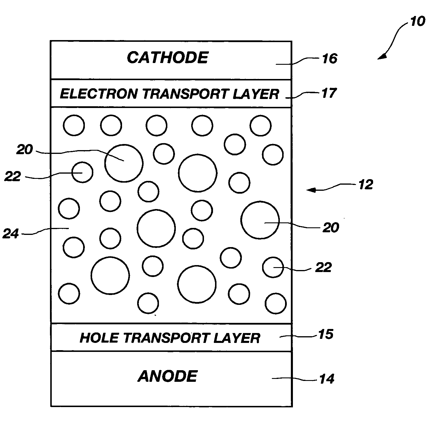
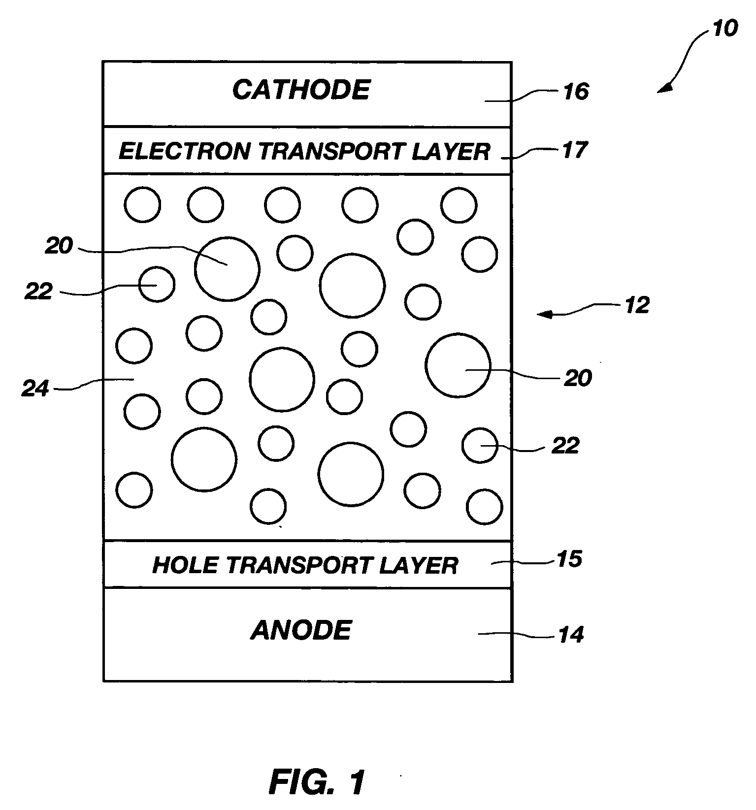
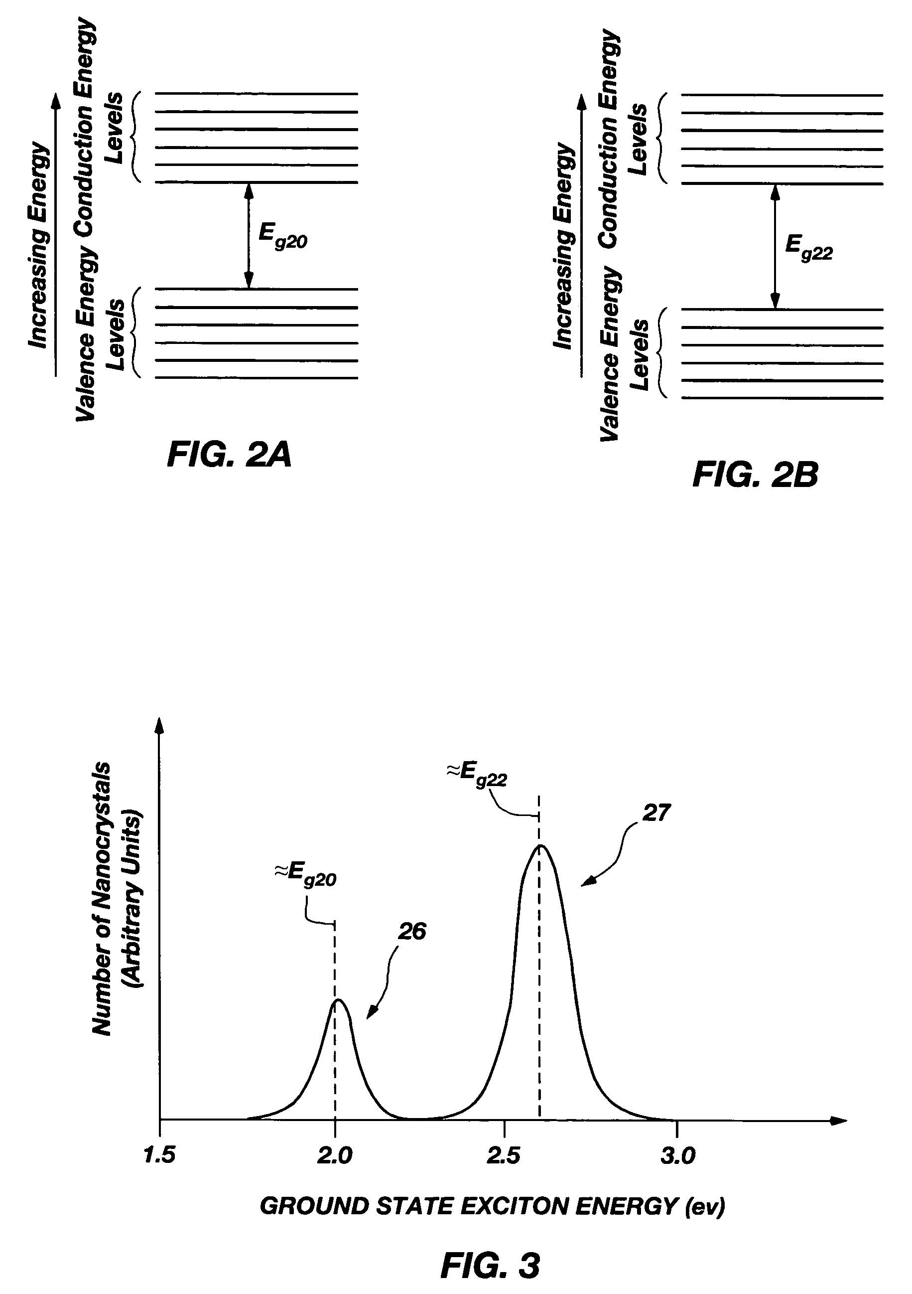
[0023]As used herein, the term “nanoparitcle” means a particle of matter that has cross-sectional dimensions of less than about 100 nanometers. The term “nanocrystal” means a nanoparticle that has a generally crystalline atomic structure. The term “luminescent nanocrystal” means a nanocrystal that is capable of emitting electromagnetic radiation upon stimulation. The term “luminescence efficiency” means the ratio of the power emitted from a luminescent material as electromagnetic radiation in a desired range of wavelengths to the power applied to the luminescent material to stimulate luminescence. The power applied to the luminescent material may be applied by, for example, electrical stimulation or optical pumping.

[0024]As used herein, the term “high energy nanocrystal” is a relative term meaning a nanocrystal that exhibits a bandgap energy that is higher relative to a “low energy nanocrystal.” The term “low energy nanocrystal” is a relative term meaning a nanocrystal that exhibits...


PUM

PropertyMeasurementUnit
Diameteraaaaaaaaaa
Diameteraaaaaaaaaa
Particle sizeaaaaaaaaaa

Abstract

Luminescent materials include a plurality of nanocrystals. At least some of the nanocrystals may be configured to emit electromagnetic radiation upon stimulation, and the plurality of nanocrystals may exhibit a multi-modal energy level distribution. The distribution of the nanocrystals may be selectively configured to enhance the luminescence efficiency of a fraction of the plurality of nanocrystals that exhibits one energy level mode of the multi-modal energy level distribution. Light-emitting diodes and electronic devices include such luminescent materials.

Description

FIELD OF THE INVENTION[0001]The present invention relates to luminescent materials (including electroluminescent materials and photoluminescent materials), luminescent devices such as, for example, light-emitting diodes, and electronic devices including luminescent materials or luminescent devices. More particularly, the present invention relates to luminescent materials that include luminescent nanocrystals dispersed throughout a material, to organic light-emitting diodes (OLED's) including such materials, and to electronic devices that include such luminescent materials or OLED's. The present invention further relates to methods for enhancing the luminescence efficiency of luminescent materials that include nanocrystals.BACKGROUND OF THE INVENTION[0002]Display devices are used to display graphical images in electronic devices including, for example, televisions, computer monitors, laptop computers, handheld computers, portable DVD players, digital music players, and other portable...

Claims


Application Information

Patent Timeline
IPC IPC(8): H01L29/08H01J1/62B32B19/00
CPCB82Y20/00B82Y30/00C09K11/02C09K11/025G02F2202/36H05B33/14H01L51/0039H01L51/502H01L51/5036H01L51/5048H01L51/0038H10K85/114H10K85/115H10K50/115H10K50/125H10K50/14C09K11/04B82B3/00
Inventor GIBSON, GARY A.SHENG, XIA
Owner HEWLETT PACKARD DEV CO LP
Why Eureka
Try Eureka