Method for melting semiconductor wafer raw material and crystal growing method for semiconductor wafer

a technology of semiconductor wafers and crystal growth methods, which is applied in the direction of polycrystalline material growth, crystal growth process, polycrystalline material growth, etc., can solve the problems of difficult technique, difficulty in achieving crystal quality, and cut wafers may have bubble-shaped defects, etc., to achieve the effect of reducing the number of pinhole defects and reducing the amount of gas bubbles in the mel

Active Publication Date: 2008-01-17
SUMCO TECHXIV
View PDF9 Cites 23 Cited by
  • Summary
  • Abstract
  • Description
  • Claims
  • Application Information

AI Technical Summary

Benefits of technology

[0029]The eleventh aspect of the invention provides a method for preventing the gas bubbles from being taken into the crystal, by rotating single crystal at a speed of 13 rpm or faster, when a single crystal is pulled up from the melt formed in the first invention or the fourth invention.
[0030]According to the present invention, the amount of heat applied to the crucible bottom part may be rendered greater than the amount of heat

Problems solved by technology

However, those cut wafers may have bubble-shaped defects, which is called the pinhole defect.
Although the technique disclosed in the above Patent Literatures 1 and 2 is directed to controlling the pressure in the furnace to reduce the pinhole defects,

Method used


Image

  • Method for melting semiconductor wafer raw material and crystal growing method for semiconductor wafer
  • Method for melting semiconductor wafer raw material and crystal growing method for semiconductor wafer
  • Method for melting semiconductor wafer raw material and crystal growing method for semiconductor wafer

Examples


first embodiment

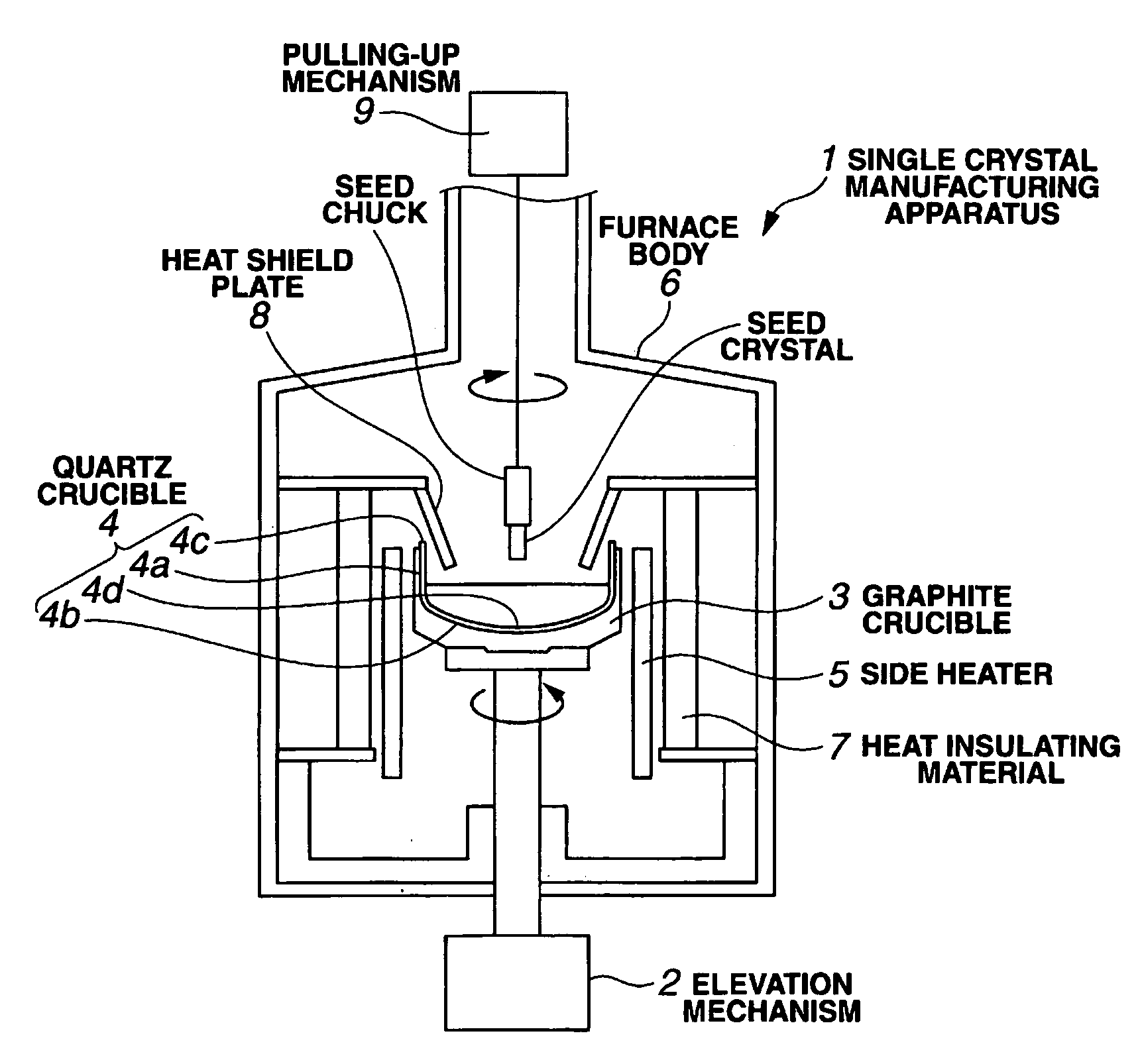
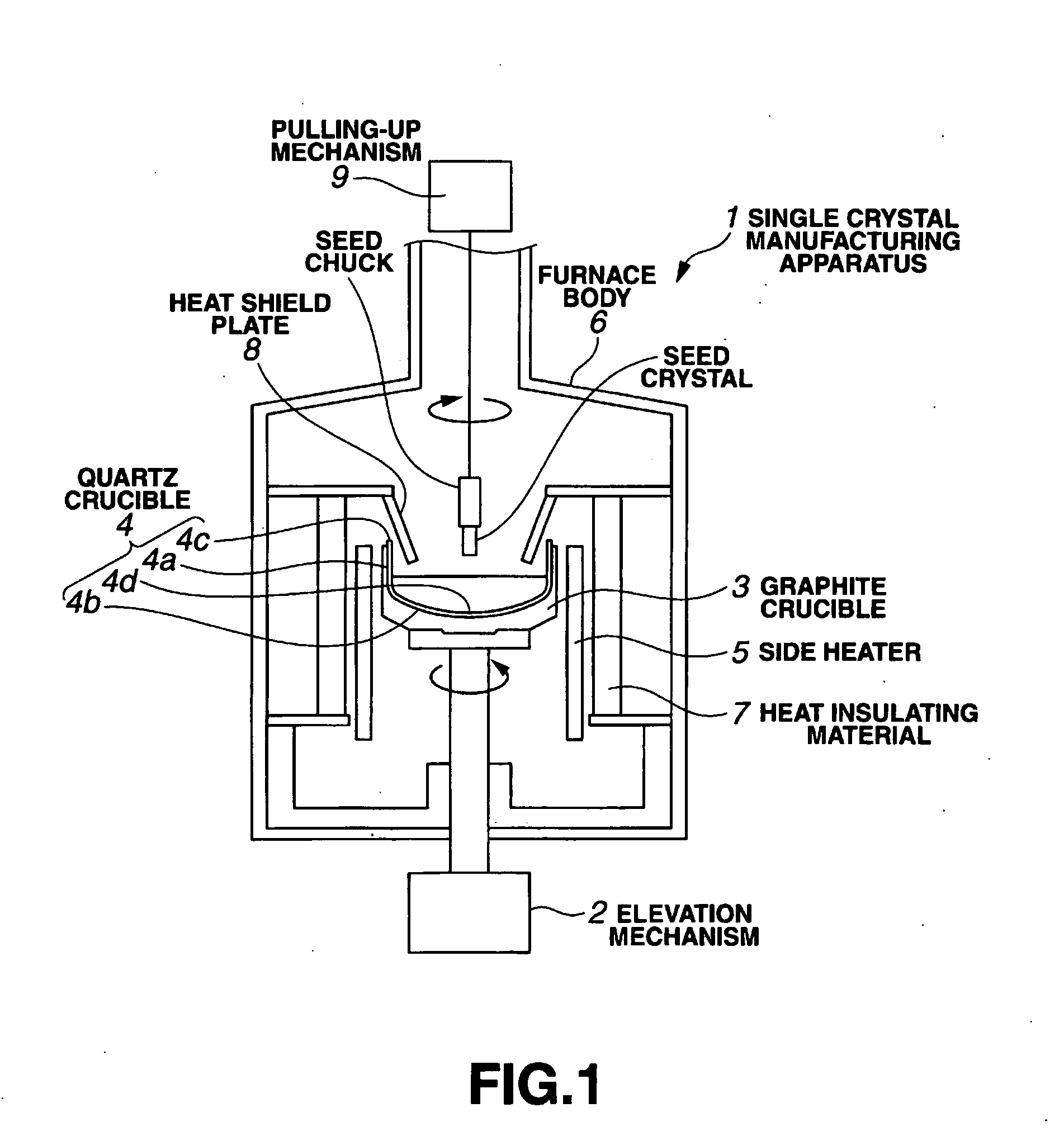
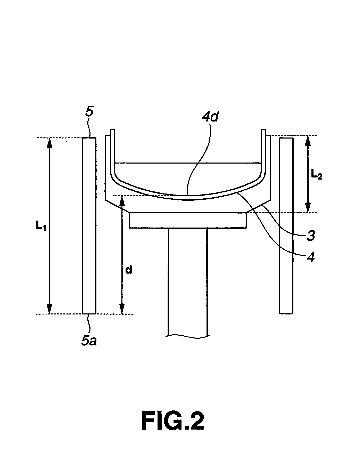
[0044]After putting lumps of silicon raw material 30 into the inside of the quartz crucible 4, the elevation mechanism 2 is operated to locate the graphite crucible 3 and the quartz crucible 4 in the initial position. At this time, as shown in FIG. 3A, the graphite crucible 3 and the quartz crucible 4 are located such that the quartz crucible bottom part 4b is positioned below the heat center. Hereinafter, the wording “graphite crucible 3 and the quartz crucible 4” is referred to as the “quartz crucible 4 and the like”. In this position, the quartz crucible 4 and the like are held, while the side heater 5 is activated to heat the quartz crucible side surface 4a through the graphite crucible 3. Then, the raw material 30 in the quartz crucible 4 is melted, resulting in a melt 31 being formed. This melt 31 contains gas bubbles which can cause pinhole defects.

[0045]After the raw material 30 in the quartz crucible 4 is all melted, the elevation mechanism 2 is operated to raise the quartz...

second embodiment

[0048]Second Embodiment is different from First Embodiment in the timing at which the quartz crucible 4 and the like are raised.

[0049]After putting lumps of silicon raw material 30 into the inside of the quartz crucible 4, the elevation mechanism 2 is operated to locate the graphite crucible 3 and the like in the initial position. At this time, as shown in FIG. 3A, the graphite crucible 3 and the like are located such that the quartz crucible bottom part 4b is positioned below the heat center. In this position, the quartz crucible 4 and the like are held, while the side heater 5 is activated to heat the quartz crucible side surface 4a. Then, the raw material 30 inside in the quartz crucible 4 is melted, resulting in a melt 31 being formed. This melt 31 contains gas bubbles which can cause pinhole defects.

[0050]After a part of the raw material 30 in the quartz crucible 4 is melted, the elevation mechanism 2 is operated to raise the quartz crucible 4 and the like. In Second Embodiment...

third embodiment

[0057]In the present embodiment, the initial position of the quartz crucible 4 is set as high as possible, and the quartz crucible 4 and the like are raised before the raw material is melted.

[0058]After putting lumps of silicon raw material 30 into the inside of the quartz crucible 4, the elevation mechanism 2 is operated to dispose the graphite crucible 3 and the like in the initial position. At this time, the graphite crucible 3 and the like are located such that the quartz crucible bottom part 4b is positioned above the heat center. The quartz crucible 4 and the like are held in this position while the side heater 5 is activated to heat the quartz crucible bottom part 4b. Then, the raw material 30 inside in the quartz crucible 4 is melted, resulting in a melt 31 being formed.

[0059]According to the present embodiment, from the initial stage of melting the material, the amount of heat applied to the crucible bottom part may be made greater than the amount of heat applied to the cru...


PUM


Abstract

The crucible and the side heater are held in the respective initial positions, and the raw material is put into the crucible. These initial positions are positions where the crucible side surface is mainly heated by the side heater. When the side heater heats the crucible side surface, the raw material is melted to form melt. When a part or all of the raw material is melted, the crucible is raised from the initial position or the side heater is lowered from the initial position. At this time, the position of the crucible or the side heater is adjusted such that the amount of heat applied to the lower side curved portion of the crucible side surface is greater than that in the initial relative position between the crucible and the side heater. And, if the crucible bottom part is heated by the side heater while the relative positions of the crucible and the side heater is maintained, the amount of heat applied to the crucible bottom part is increased as compared to the amount of heat applied to the crucible side surface, and the convection in the melt that makes the gas bubbles spatter to the outside. In this way, the gas bubbles are eliminated from the melt. As a result, the amount of gas bubbles in the melt can be reduced without deforming the crucible, and occurrence of pinhole defects in the wafer can be suppressed.

Description

BACKGROUND OF THE INVENTION[0001]1. Field of the Invention[0002]The present invention relates to a method for melting semiconductor wafer raw material, in which the semiconductor wafer raw material is placed in a crucible of a single crystal manufacturing apparatus, and is melted by heating the crucible with a side heater, and particularly relates to a melting method for semiconductor wafer raw material that uses a side heater to heat the crucible bottom part to reduce the amount of gas bubbles in the melt.[0003]2. Description of the Related Art[0004]To manufacture the single crystal silicon using the single crystal manufacturing device, chunks of polycrystalline as raw material are put into the quartz crucible. The side surface of the crucible is then heated using the side heater that is arranged so as to surround the side of the crucible. As the material has been melted, the silicon melt is generated. On the tip of a crystal pulling mechanism disposed in an upper part of the cruci...

Claims


Application Information

Patent Timeline
IPC IPC(8): C30B15/14
CPCC30B15/14C30B11/003C30B29/06C30B35/00Y10T117/1068
Inventor SHIMOMURA, KOICHIKOTOURA, EIICHIROUOHTA, HIROYUKI
Owner SUMCO TECHXIV
Why Eureka
Try Eureka