System and method for low voltage booster circuits

a booster circuit and low-voltage technology, applied in the field of low-voltage booster circuits, can solve the problems of high current consumption, more heat and noise in the chip, etc., and achieve the effect of reducing current consumption and reducing current consumption

Inactive Publication Date: 2008-01-17
SANDISK TECH LLC
View PDF11 Cites 31 Cited by
  • Summary
  • Abstract
  • Description
  • Claims
  • Application Information

AI Technical Summary

Benefits of technology

[0007]In one aspect of the present invention, a method of reducing current consumption in a low voltage booster circuit is provided. The method includes the steps of (a) enabling an input signal to activate plural out of phase clocks; and (b) disabling the input signal after a pre-determined time and after an output voltage has reached a certain level.
[0008]In another aspect of the present invention, a system for reducing current consumption in a low voltage booster circuit is provided. The system includes a clock doubler circuit; a high voltage stage circuit, having an output voltage, connected to the clock doubler circuit, wherein an input signal to the clock doubler circuit activates plural out of phase clocks when the input signal is enabled; and the input signal is disabled after a pre-determined time and after the output voltage has reached a certain level.

Problems solved by technology

Although the low voltage booster circuit provides a fast ramp up time, it also has the undesirable side effect of high current consumption which generates more heat and more noise in the chip.
The high current consumption is a result of two internal capacitors in the low voltage booster circuit that are used to amplify clock signals.

Method used


Image

  • System and method for low voltage booster circuits
  • System and method for low voltage booster circuits
  • System and method for low voltage booster circuits

Examples


Embodiment Construction

[0019]To facilitate an understanding of the preferred embodiment, the general architecture and operation of a low voltage booster circuit will be described. The specific architecture and operation of the preferred embodiment will then be described with reference to the general architecture.

General Description of a Local Booster Circuit Structure

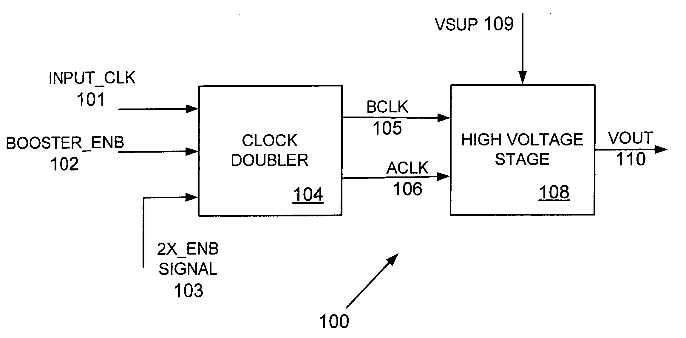
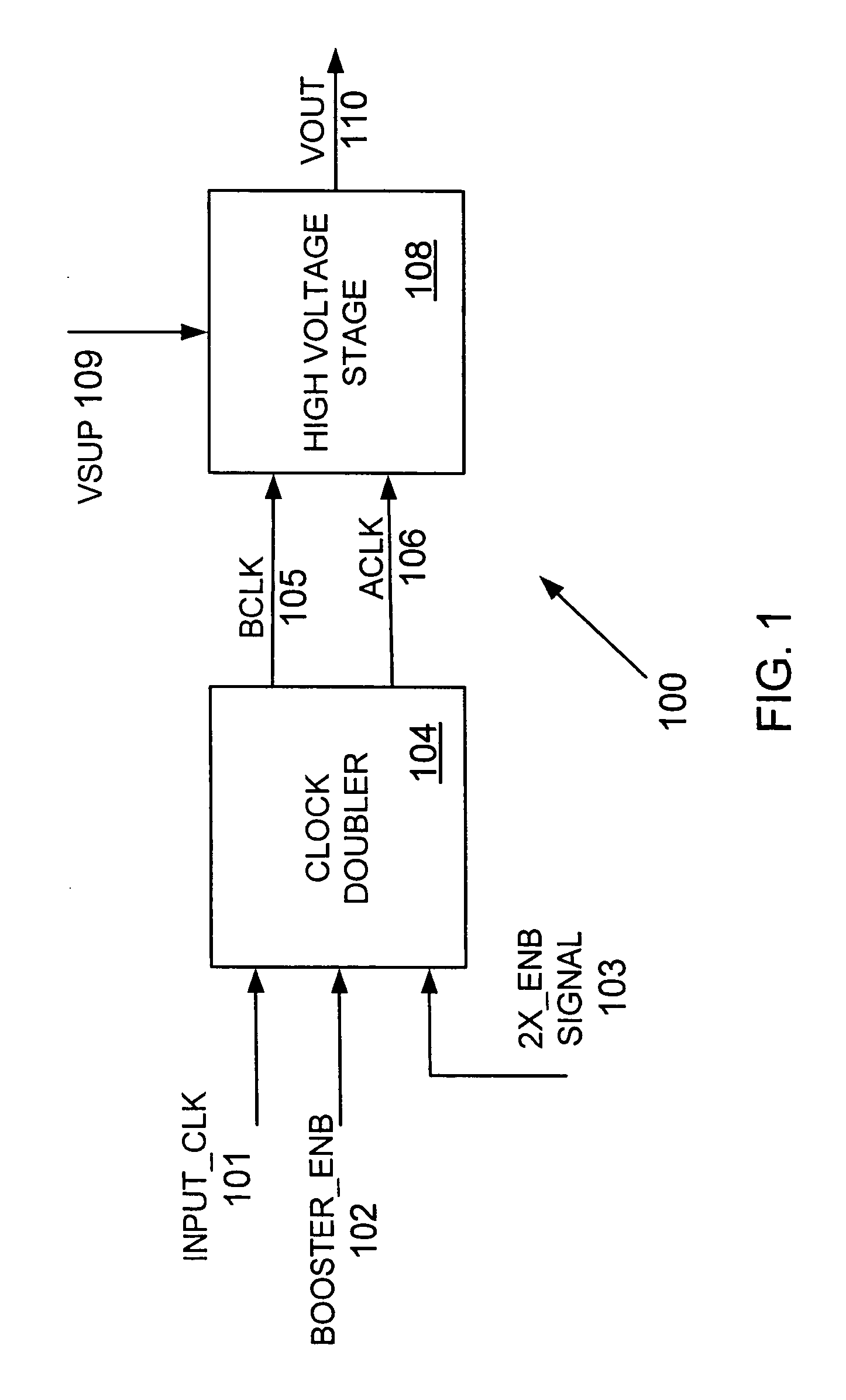
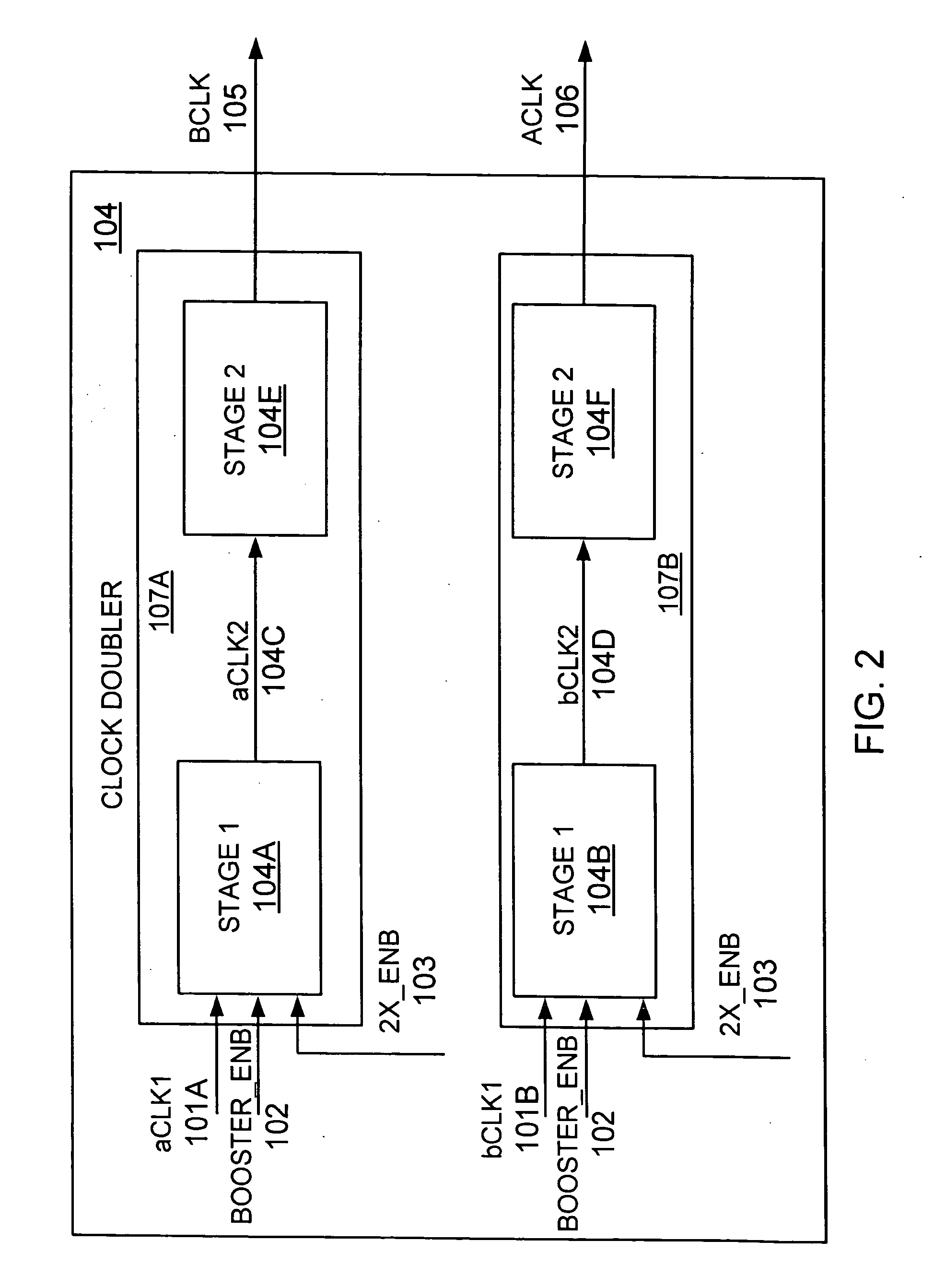
[0020]A typical low voltage booster circuit 100 is shown in FIG. 1. Low voltage booster circuit 100 is comprised of a clock doubler circuit 104 connected to a high voltage stage circuit 108. An output voltage VOUT 110 is generated from low voltage booster circuit 100 based on output clock signals, BCLK 105 and ACLK 106, from clock doubler circuit 104 and an input voltage VSUP 109.

[0021]Clock doubler circuit 104 receives a clock signal INPUT_CLK 101, an input signal BOOSTER_ENB 102 and an input signal 2X_ENB 103. When BOOSTER_ENB signal 102 and 2X_ENB signal 103 are high, all clock signals within clock doubler circuit 104 are activated and out...


PUM


Abstract

A system and method of reducing current consumption in a low voltage booster circuit is provided. The method includes the steps of (a) enabling an input signal to activate plural out of phase clocks; and (b) disabling the input signal after a pre-determined time and after an output voltage has reached a certain level.

Description

BACKGROUND[0001]1. Field of the Invention[0002]The present invention is related to non-volatile memory devices (“flash memory devices”), and more particularly, to low voltage booster circuits used in flash memory devices.[0003]2. Background[0004]Semiconductor memory devices have become popular for use in various electronic devices. For example, non-volatile semiconductor memory is used in cellular telephones, digital cameras, personal digital assistants, mobile computing devices, non-mobile computing devices and other electronic devices. Electrical Erasable Programmable Read Only Memory (EEPROM) and flash memory are among the most popular non-volatile semiconductor memories.[0005]Flash memory devices are comprised of an array of memory cells that are selected by word lines extending along rows of the memory cells, and bit lines extending along columns of the memory cells. Low voltage booster circuits are used to generate a voltage level higher than a given input voltage and the gene...

Claims


Application Information

Patent Timeline
Patent Type & Authority Applications(United States)
IPC IPC(8): G05F1/10
CPCG11C5/145H02M3/073G11C16/12
Inventor KATO, YOSUKE
Owner SANDISK TECH LLC
Why Eureka
Try Eureka