Semiconductor device and manufacturing process therefor
- Summary
- Abstract
- Description
- Claims
- Application Information
AI Technical Summary
Benefits of technology
Problems solved by technology
Method used
Image

Examples
embodiment 1
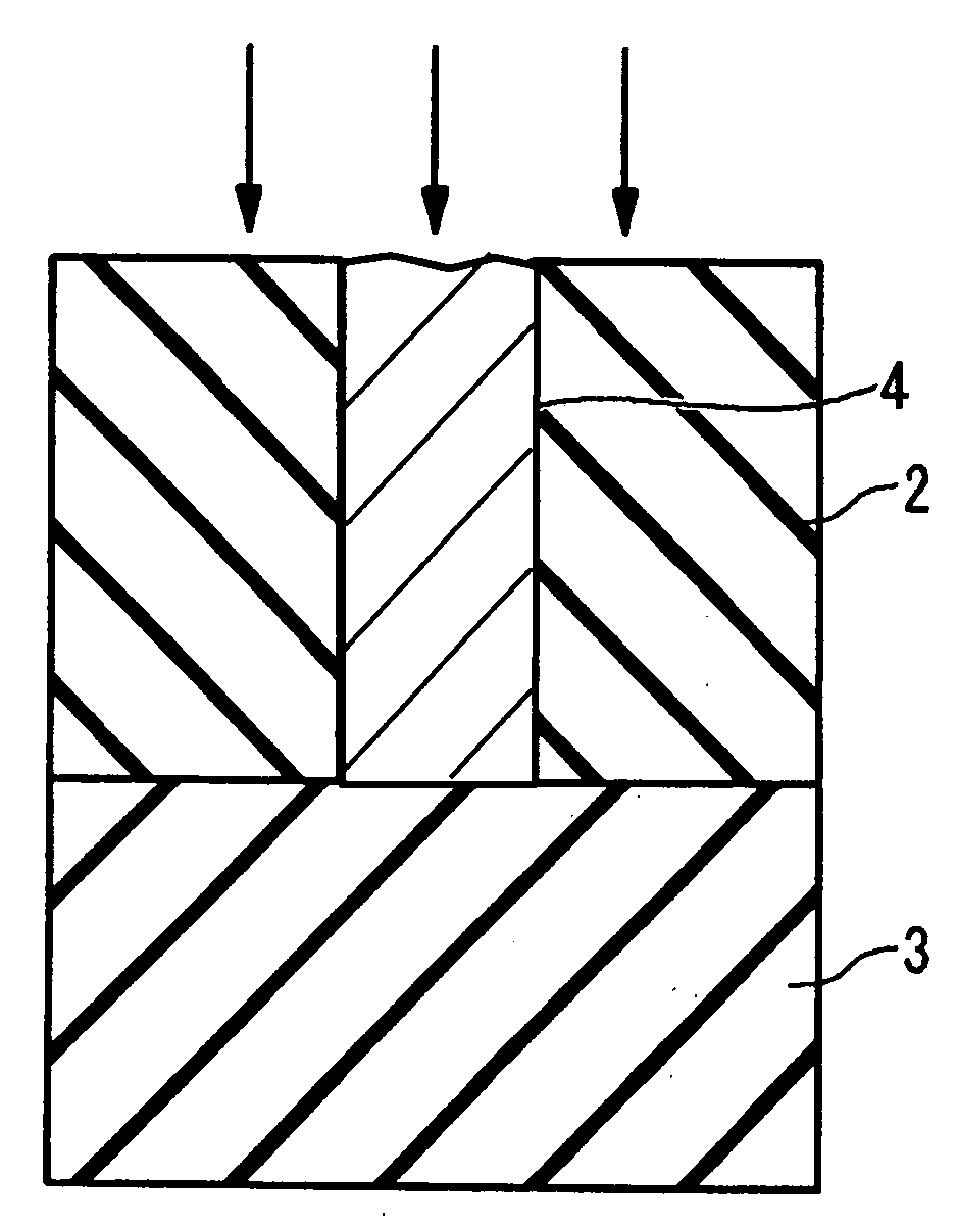
[0052]There will be described Embodiment 1 where the present invention is applied to a semiconductor device 100 comprising a DRAM with reference to the drawings. First, a DRAM memory cell will be outlined with reference to FIGS. 19 and 20. FIG. 19 shows a plan view of a memory cell and FIG. 20 shows a cross-sectional view taken on line B-B in FIG. 19. In these figures, identical components are indicated by the same symbols.
[0053]First, see the plan view of FIG. 19. Each component in the layout illustrated in FIG. 19 is formed on a semiconductor substrate 3. For ease of explanation, the structures, which cannot be seen because of interruption by an interlayer insulating film and so on, are made visible by perspective representation. On the semiconductor substrate 3, there are formed a plurality of active regions 101 surrounded by element separating regions 90. There are formed a plurality of word lines (gate electrodes) 102 such that they traverse longitudinally the plurality of acti...
embodiment 2
[0074]There will be described Embodiment 2. FIG. 22 is a flow chart of a manufacturing process for a semiconductor device according to this embodiment. In this embodiment, the shape of the polysilicon plug 4 during hydrogen annealing is modified in comparison with Embodiment 1. Furthermore, this embodiment will be described for the case of forming another polysilicon plug instead of a tungsten plug on the polysilicon plug 4 as in Embodiment 1.
Step S1, 2: Formation of a Contact Hole and Deposition of Polysilicon
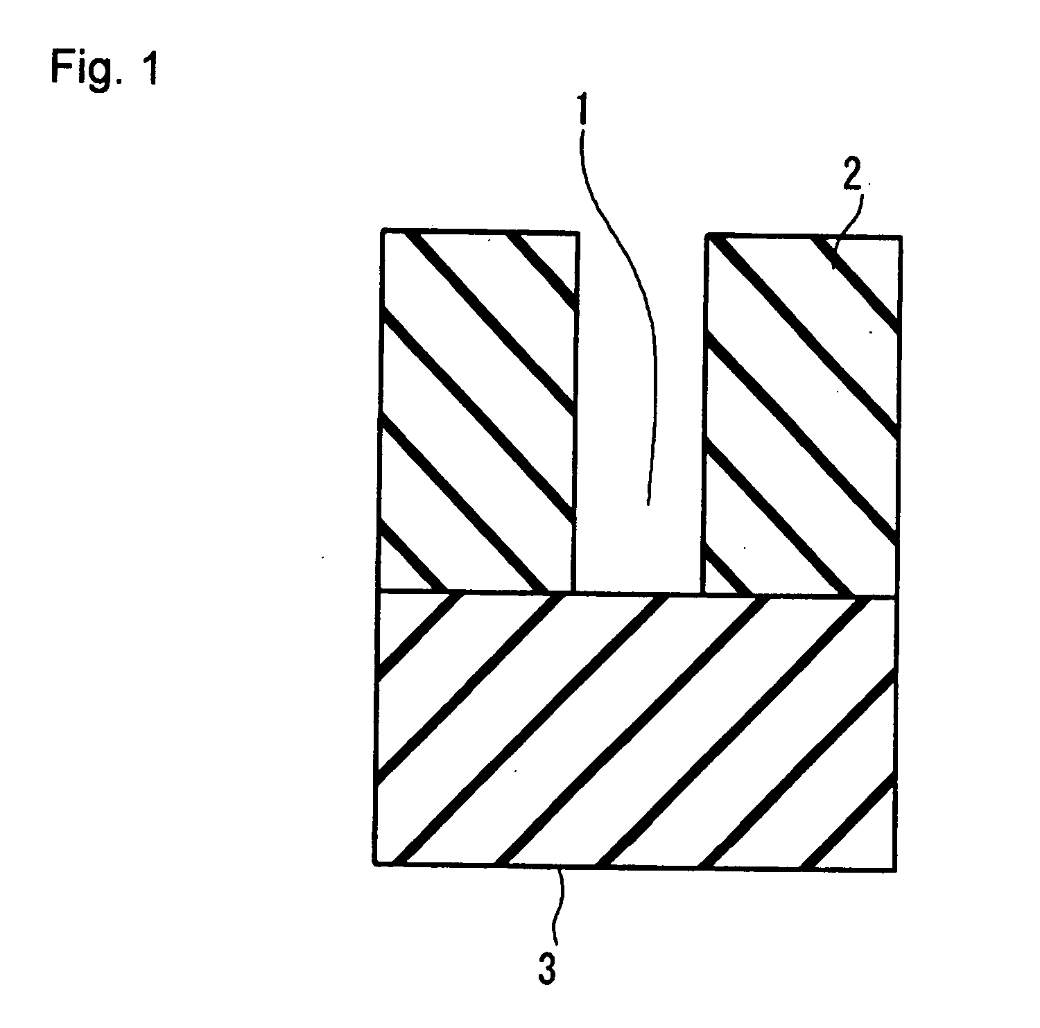
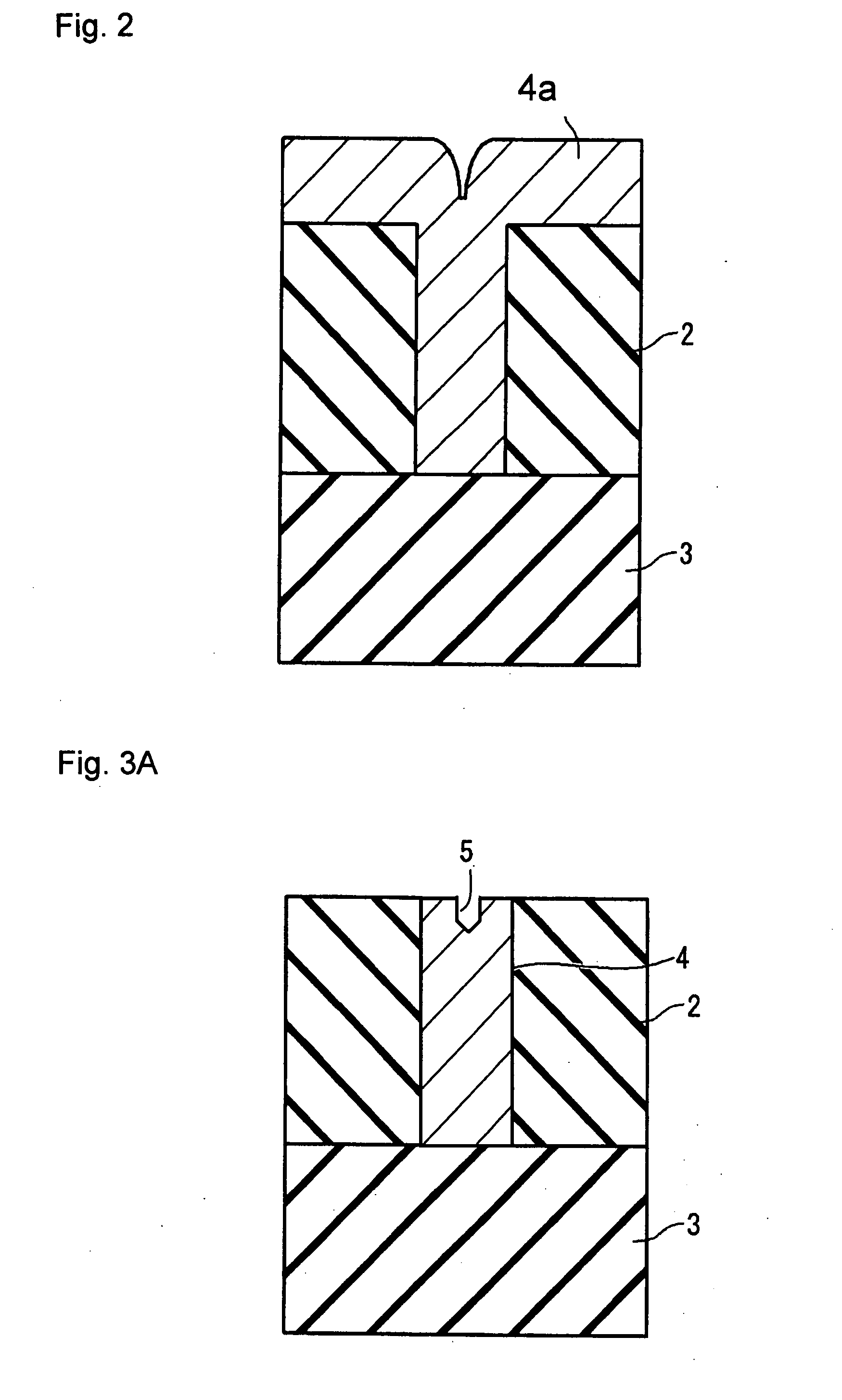
[0075]As described in Embodiment 1, a contact hole 1 is formed (S1) and a polysilicon 4a is deposited (S2).
Step S3-1: Etching Back of Polysilicon
[0076]As described in Embodiment 1, the polysilicon 4a deposited on the region other than the contact hole 1 was removed by etching back to form a polysilicon plug 4.
Step S3-4: Etching Back of a Silicon Oxide Film
[0077]First, see FIGS. 10A, B. After forming the contact plug 4, part of the silicon oxide film 2 surrounding the contact p...
embodiment 3
[0084]There will be described Embodiment 3. FIG. 23 is a flow chart of a manufacturing process for a semiconductor device according to this embodiment. In this embodiment, processing is conducted such that the upper surface of the polysilicon plug 4 is within a contact hole and has a concave shape. In comparison with Embodiments 1 and 2, it is modified in that silicon is selectively epitaxially grown. Each step will be described.
Step S1, 2: Formation of a Contact Hole and Deposition of Polysilicon
[0085]As described in Embodiment 1, a contact hole 1 is formed (S1) and a polysilicon 4a is deposited (S2).
Steps S3-1 to 3-5: Processing of Polysilicon into a Concave Shape and Selective Epitaxial Growth
[0086]See FIGS. 14A, B. As described in Embodiment 1, the polysilicon 4a is etched back to form a polysilicon plug 4 (S3-1). Then, a silicon oxide film 24 to be an interlayer insulating film is deposited by plasma CVD using TEOS as a starting material (S3-2). Next, a hole is formed in the si...
PUM
 Abstract
Description
Claims
Application Information
 - Generate Ideas
- Intellectual Property
- Life Sciences
- Materials
- Tech Scout
- Unparalleled Data Quality
- Higher Quality Content
- 60% Fewer Hallucinations
Browse by: Latest US Patents, China's latest patents, Technical Efficacy Thesaurus, Application Domain, Technology Topic, Popular Technical Reports.
© 2025 PatSnap. All rights reserved.Legal|Privacy policy|Modern Slavery Act Transparency Statement|Sitemap|About US| Contact US: help@patsnap.com