

Semiconductor device encapsulated by silicone resin composition, and silicone resin tablet for encapsulating semiconductor device
a technology of silicone resin and semiconductor, which is applied in the direction of semiconductor devices, solid-state devices, semiconductor/solid-state device details, etc., can solve the problems of insufficient impact strength, insufficient crack generation, and still suffer from surface tackiness and dust deposition, etc., to achieve excellent flexibility, reduce surface tackiness, and high reliability
- Summary
- Abstract
- Description
- Claims
- Application Information
AI Technical Summary
Benefits of technology
Problems solved by technology
Method used
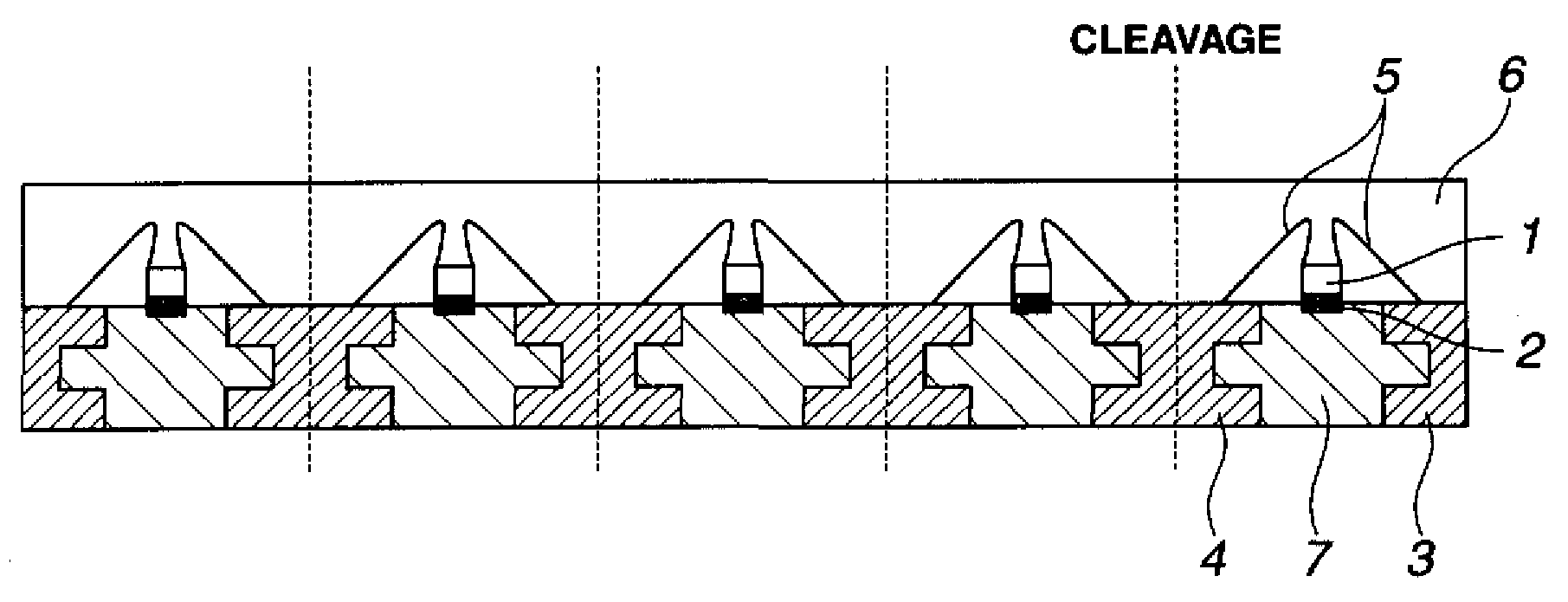
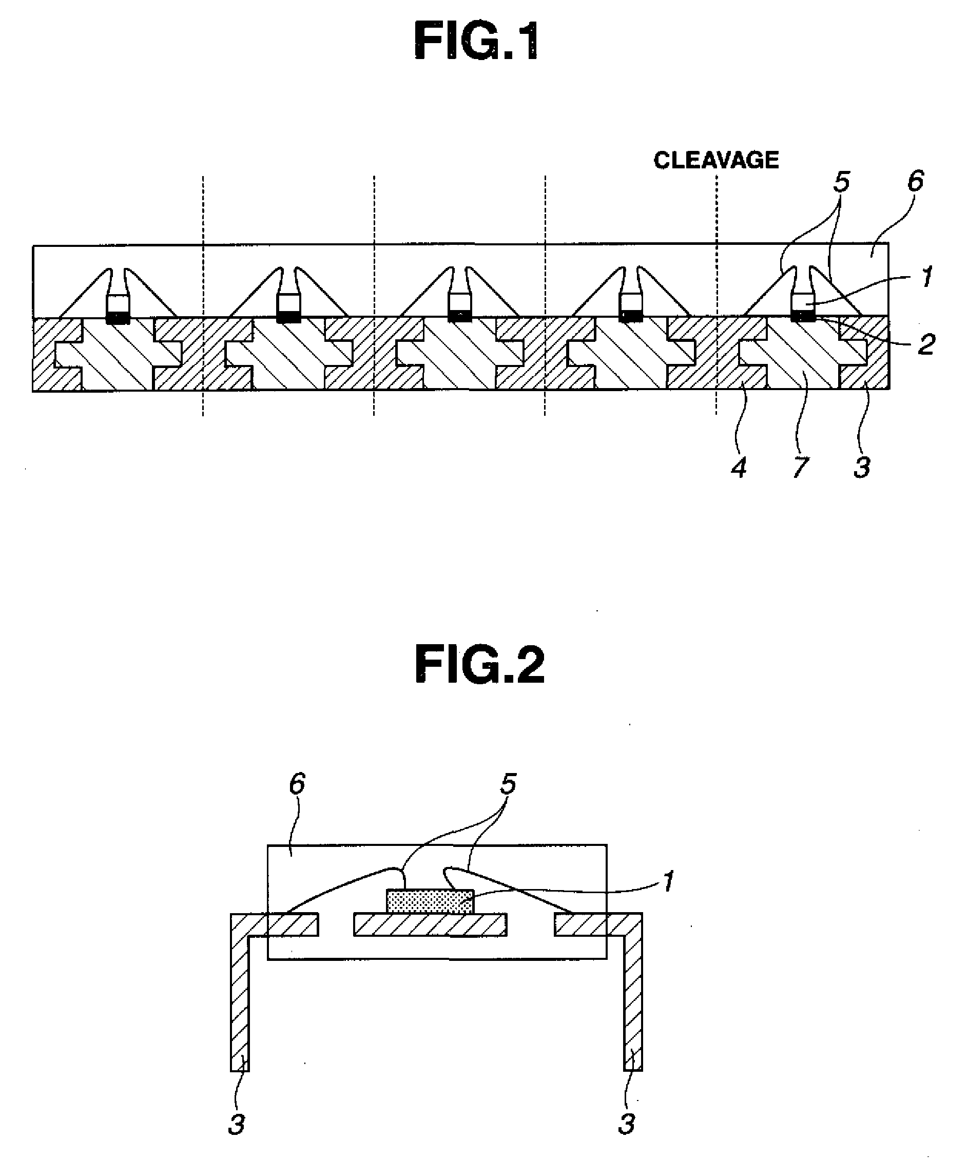
Image

Examples
synthesis example 1
[0086]27 moles of an organosilane represented by PhSiCl3, 1 mole of ClMe2SiO(Me2SiO)33SiMe2Cl, and 3 moles of MeViSiCl2 were dissolved in toluene solvent, and the solution was added dropwise to water for simultaneous hydrolysis. After washing the reaction mixture with water and neutralizing by washing with an alkali, the water was removed, and the solvent was stripped to synthesize vinyl group-containing resin. This resin had a weight average molecular weight of 62,000 and a melting point of 60° C.
synthesis example 2
[0087]27 moles of an organosilane represented by PhSiCl3, 1 mole of ClMe2SiO(Me2SiO)33SiMe2Cl, and 3 moles of MeHSiCl2 were dissolved in toluene solvent, and the solution was added dropwise to water for simultaneous hydrolysis. After washing the reaction mixture with water and neutralizing by washing with an alkali, the water was removed, and the solvent was stripped to synthesize hydrosilyl group-containing resin. This resin had a weight average molecular weight of 58,000 and a melting point of 58° C.
synthesis example 3
[0088]27 moles of an organosilane represented by PhSiCl3, 1 mole of ClMe2SiO(Me2SiO)33SiMe2Cl, and 3 moles of Me2ViSiCl were dissolved in toluene solvent, and the solution was added dropwise to water for simultaneous hydrolysis. After washing the reaction mixture with water and neutralizing by washing with an alkali, the water was removed, and the solvent was stripped to synthesize vinyl group-containing resin. This resin had a weight average molecular weight of 63,000 and a melting point of 63° C.
PUM
| Property | Measurement | Unit |
|---|---|---|
| elongation | aaaaa | aaaaa |
| molar ratio | aaaaa | aaaaa |
| molar ratio | aaaaa | aaaaa |
Abstract
Description
Claims
Application Information