
Solar cell module

a solar cell and module technology, applied in the field of solar cell modules, can solve the problems of long time exposure to the outside air, no study on weather resistance such as moisture resistance, and no study on weather resistance, etc., and achieve the effect of excellent conductivity and easy acquisition of light transmittan

Inactive Publication Date: 2008-01-31
SANYO ELECTRIC CO LTD
View PDF4 Cites 29 Cited by
  • Summary
  • Abstract
  • Description
  • Claims
  • Application Information

AI Technical Summary

Benefits of technology

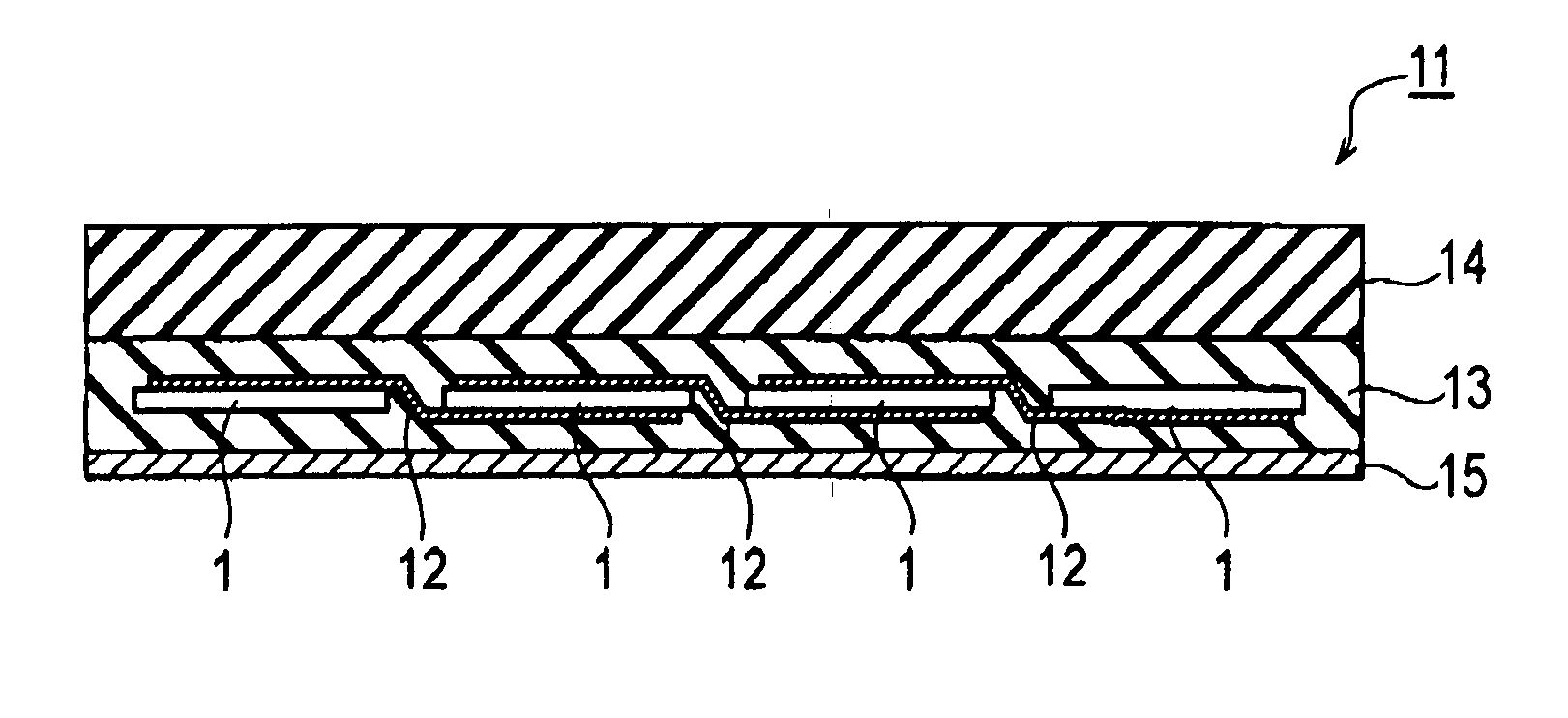
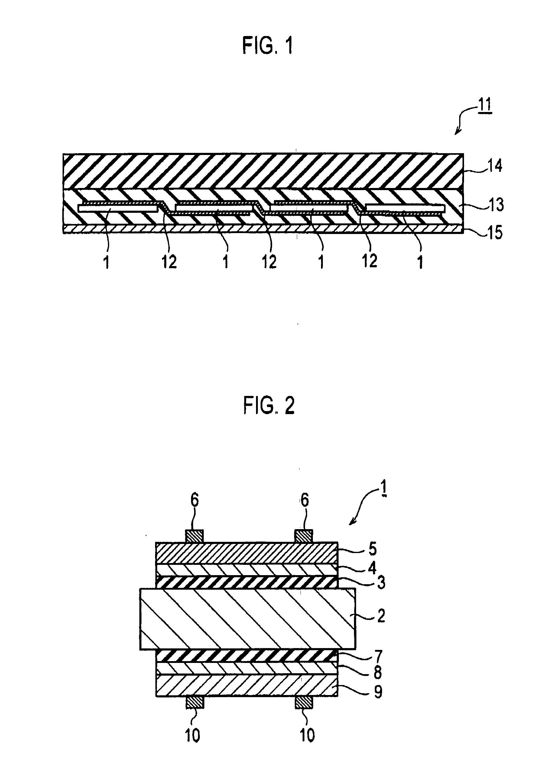
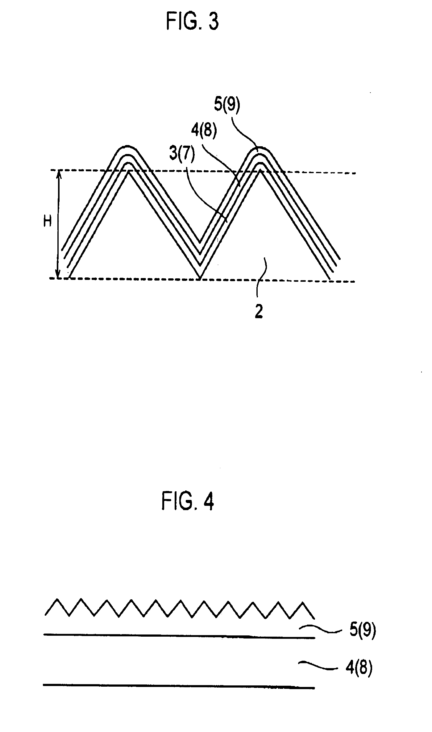
[0011] According to the solar cell module of the above-described invention, the arithmetic mean roughness of the first transparent conductive film disposed above the back surface side protective member of the photovoltaic element is made larger than that of the second transparent conductive film disposed above the light receiving surface side protective member, so that a weather resistance on the side of the first transparent conductive film can be increased than that on the side of the second transparent conductive film. It is therefore possible to reduce an influence of moisture on a property of the photovoltaic element, the moisture permeating through the back surface side protective member and entering the solar cell module. The arithmetic mean roughness of the second transparent conductive film disposed above the side of the light receiving surface side protective member can be made smaller than that of the first transparent conductive film disposed above the side of the back surface side protective member, so that the light transmittance and conductivity of the second transparent conductive film can be more enhanced than those of the first transparent conductive film. Thus, light which permeates through the light receiving surface side protective member and which enters the solar cell module can be effectively brought into the photovoltaic element, and concurrently a resistance loss can be also made small which loss occurs when taking out a light generation carrier generated in the photovoltaic element through the second transparent conductive film. As described above, a solar cell module having a high output and an excellent weather resistance can be provided.
[0013] According to the above-described solar cell module, a further enhancement of the weather resistance can be achieved by using the indium oxide that is not easily dissolved into water.
[0015] According to the above-described solar cell module, an excellent weather resistance can be obtained.
[0017] According to the above-described solar cell module, since the first transparent conductive film is formed of tungsten doped indium oxide tungsten, the arithmetic mean roughness (Ra) can made small, and additionally since the arithmetic mean roughness (Ra) is 1.0 nm or less, the conductivity and light transmittance along with the weather resistance can be enhanced.
[0019] According to the above-described solar cell module, since the second transparent conductive film is formed of indium oxide to which tungsten is added, the arithmetic mean roughness (Ra) can made small, and additionally since the arithmetic mean roughness (Ra) is 0.5 nm or less, the conductivity and light transmittance can be further enhanced.
[0021] According to the above-described solar cell module, the amorphous semiconductor layer exists between the crystalline semiconductor layer and the first transparent conductive film, so that the first transparent conductive film is formed without being influenced by the orientation of the crystalline semiconductor layer. Thus, the arithmetic mean roughness (Ra) of the first transparent conductive film is optimally controlled, and the first transparent conductive film having excellent conductivity and light transmittance can be easily obtained.

Problems solved by technology

On the other hand, when mounting a photovoltaic element on a solar cell module, there is high possibility that it is open to the outside air for a long period.
However, no study has been made on weather resistance such as moisture resistance under the above condition.

Method used


Image

  • Solar cell module
  • Solar cell module
  • Solar cell module

Examples


example

[0082] Although a photovoltaic element according to the present invention is specifically described below with reference to an example, the present invention is not limited to the following example, and various changes may be made therein without departing from the spirit of the present invention.

(Relationship Between Arithmetic Mean Roughness and Pressure)

[0083] First, to investigate a relationship between pressure of forming an indium oxide layer and an arithmetic mean roughness (Ra), pressure applied when forming an indium oxide layer is changed, and the arithmetic mean roughness (Ra) on a surface of the indium oxide layer is measured. To be more precise, a sintered body of In2O3 powder in which 3 weight percent of WO3 powder is mixed is used as a target, whereby an indium oxide layer is formed on a mirror silicon substrate by an ion plating method. In this manner, the mixing-in of the WO3 powder enables the value of Ra to be smaller than that obtained when mixing SnO2 or the ...


PUM


Abstract

A solar cell module includes a photovoltaic element, a light receiving surface side protective member disposed above a light receiving surface of the photovoltaic element, and a back surface side protective member disposed above a back surface opposite to the light receiving surface side of the photovoltaic element. The photovoltaic element includes an indium oxide layer formed on a surface facing the back surface side protective member and another indium oxide layer formed on a surface facing the light receiving surface side protective member. An arithmetic mean roughness (Ra) on a surface of the indium oxide layer on the back surface of the photovoltaic element is larger than an arithmetic mean roughness (Ra) on the light receiving surface of the photovoltaic element.

Description

CROSS REFERENCE TO RELATED APPLICATIONS [0001] This application is based upon and claims the benefit of priority from prior Japanese Patent Application No. 2006-198721, filed on Jul. 20, 2006; the entire contents of which are incorporated herein by reference. BACKGROUND OF THE INVENTION [0002] 1. Field of the Invention [0003] The present invention relates to a solar cell module which includes a photovoltaic element, a light receiving surface side protective member disposed above a light receiving surface of the photovoltaic element, and a back surface side protective member disposed above a back surface opposite to the light receiving surface of the photovoltaic element. [0004] 2. Description of the Related Art [0005] Heretofore, a photovoltaic element, which includes a transparent conductive film formed of indium oxide layers, is known. For such an indium oxide layer, ITO (Indium Tin Oxide) being In2O3 to which SnO2 is added as impurities has been widely used because of its high co...

Claims


Application Information

Patent Timeline
Patent Type & Authority Applications(United States)
IPC IPC(8): H01L31/0236H01L31/0216H01L31/04
CPCH01L31/0236H01L31/03762Y02E10/548H01L31/1884H01L31/0747H01L31/02363
Inventor NAKASHIMA, TAKESHIMARUYAMA, EIJI
Owner SANYO ELECTRIC CO LTD
Learn More